3D NAND storage device and manufacturing method thereof
A technology of storage devices and storage areas, applied in the field of flash memory, can solve the problems of increasing, the process cannot be integrated with 3D NAND devices, etc., and achieve the effect of easy process integration
- Summary
- Abstract
- Description
- Claims
- Application Information
AI Technical Summary
Problems solved by technology
Method used
Image

Examples
Embodiment 1
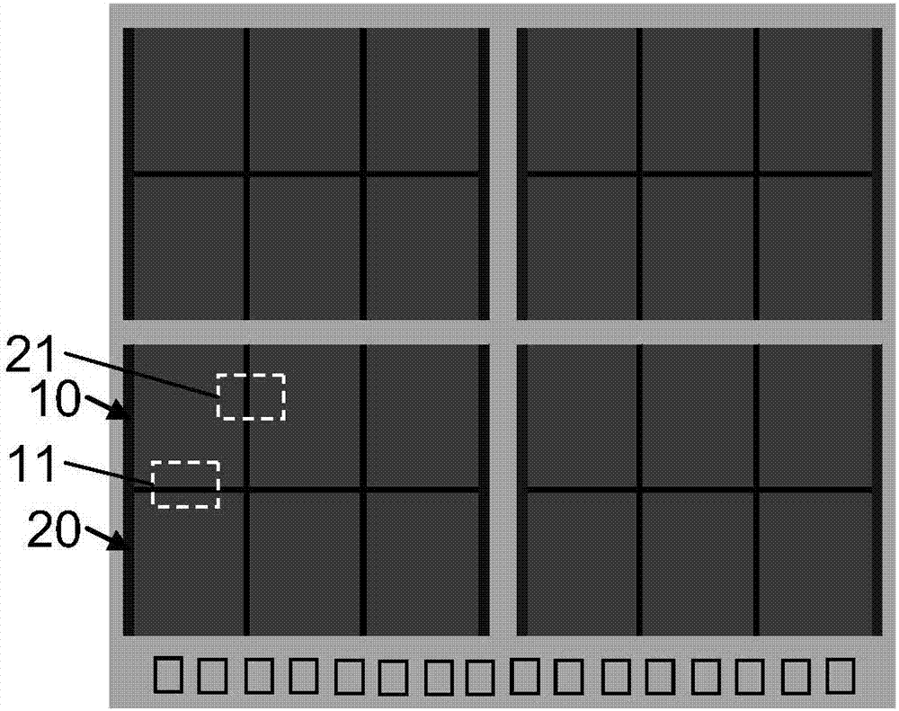
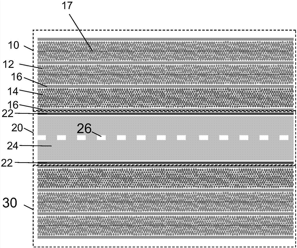
[0056] In the embodiment of the present invention, the via hole forming region 20 is arranged between two storage regions in the direction of the bit line, and the first storage region 10 and the second storage region 30 are regions for forming an array of memory cells. The design can be one or more block storage areas.
[0057] refer to figure 1 Shown is a schematic top view of a 3D NAND memory device chip according to an embodiment of the present invention. In this specific embodiment, the memory chip includes 4 plate storage areas, and in each plate (plate) storage area It includes a plurality of block storage areas, and the via hole forming area 20 is formed in the middle part of a slice storage area, and passes through the entire slice storage area along the word line direction. It can be understood that this is only an example, and there may be other design arrangements according to different designs, and the present invention is not limited thereto.
[0058] refer to ...
Embodiment 2
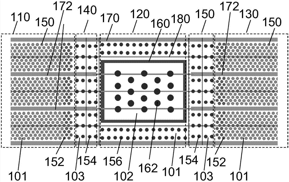
[0077] In this example, refer to image 3 As shown, the block storage areas are separated by gate line gaps 170, the direction of the gate line gaps 170 is the word line direction, the gate line gaps are parallel to each other, and the finger storage area is between a pair of gate line gaps 170. exist image 3 In the specific embodiment shown, a gate line gap divides a block storage area into three finger storage areas, which can be divided into two or more finger storage areas according to different design requirements.
[0078] As described above, refer to Figure 5As shown, the gate line gap 170 penetrates to the bottom of the stacked layer, the sidewall of the gate line gap 170 is an oxide layer, the filling material is metal, such as W, and a doped region is formed under it, which is set in the middle of the finger storage region There is a top select gate cut (Top Select Gate Cut) 180, which divides the top select gate of the storage area into two parts, and the top se...
Embodiment 3
[0085] In this embodiment, the parts different from those in the second embodiment will be described, and the same parts will not be repeated.
[0086] refer to Figure 4 As shown, a pair of gate line gaps 172 parallel to each other extending to the insulating ring 160 are formed in the block stack layers of the first region 110 and the third region 130, and the insulating ring 160 along the direction perpendicular to the gate line gaps The boundary of the slit extends at least to a region outside the pair of mutually parallel gate line gaps 170, so that the insulating ring 160 stacks the blocks of the first region 110 and the third region 130 between the pair of mutually parallel gate line gaps 172 The metal layer in the block stack is completely blocked, that is, the top select gates in the memory region on both sides of the insulating ring 160 cannot be connected through the top metal layer in the block stack layer.
[0087] In this embodiment, the outer side of the first ...
PUM
 Abstract
Description
Claims
Application Information