All-optical phase modulator

An optical phase and modulator technology, applied in optical demodulation, optics, instruments, etc., can solve the problems of inability to generate fs-level electrical pulses, difficult processes, and instability.

Active Publication Date: 2017-08-18
NANJING HENGGAO OPTO ELECTRONICS RES INST CORP
View PDF4 Cites 4 Cited by
  • Summary
  • Abstract
  • Description
  • Claims
  • Application Information

AI Technical Summary

Problems solved by technology

At present, the single-channel 40Gb / s electro-optic modulator has matured (domestic electro-optic modulators still have instability problems), but it is very difficult to further increase the single-channel rate of the electro-optic modulator (here, excluding the use of dual-channels caused by speed increase)
Because with the increase of the modulation rate, the electrical signal and the optical signal in the modulator are required to be transmitted synchronously in the form of traveling waves, and the inter-electrode capacitance must be very small, which is difficult to achieve in the process
Especially when the ultra-narrow optical pulse is at the fs level, it is almost impossible to use the electro-optic modulator to realize the fs-level optical modulation, not only cannot generate the fs-level electrical pulse, but also cannot perform electro-optic modulation

Method used


Image

  • All-optical phase modulator
  • All-optical phase modulator
  • All-optical phase modulator

Examples


Embodiment 1

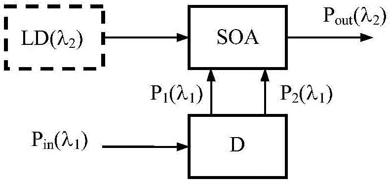
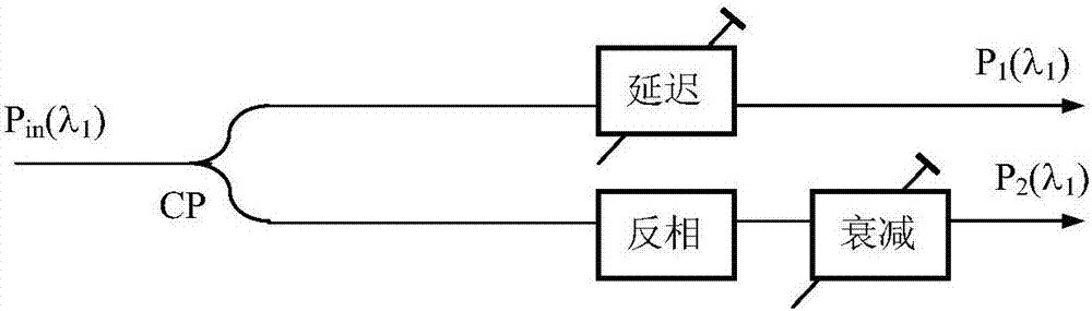
[0058] Such as Figure 7 As shown, a fast tunable all-optical phase modulator includes an optical coupler (CP), a tunable delayer, a first semiconductor optical amplifier (SOA1), a first optical filter, a tunable attenuator, a first wave A division multiplexing coupler, a local laser, a second wavelength division multiplexing coupler, a second semiconductor optical amplifier (SOA2), an optical circulator, and a second optical filter.

[0059] Among them, the wavelength from the outside of the all-optical phase modulator is λ 1 The input optical signal of the optical coupler is connected with the input end of the optical coupler, and one output end of the optical coupler is connected with the input end of the tunable delayer; the other output end of the optical coupler is connected with the first wavelength division multiplexing coupler One input end of the tunable delayer is connected with one input end of the second wavelength division multiplexing coupler; the other input e...


PUM


Abstract

The invention discloses an all-optical phase modulator which comprises a differential balance signal forming unit and an optical phase modulation unit. The optical phase modulation unit comprises a semiconductor optical amplifier; the differential balance signal forming unit is used for changing an intensity-modulated optical signal with a wavelength of lambda 1 into two paths of differential balance signals, and the two paths of differential balance signals are injected into the semiconductor optical amplifier respectively in the same direction with probe light and in a different direction with the probe light; the two paths of differential balance signals respectively are a first path of optical signal with the wavelength of lambda 1 and a second path of optical signal with a wavelength of lambda' 1 after radix-minus-one complement; the first path of optical signal and the second path of optical signal after radix-minus-one complement are reverse codes mutually; and the semiconductor optical amplifier is used for generating cross phase modulation according to interaction of two paths of differential balance signals and the probe light which needs to be modulated. The all-optical phase modulator disclosed by the invention can implement rapid tuning, and is simple in structure and convenient to use.

Description

technical field [0001] The invention relates to the technical field of phase modulators, in particular to an all-optical phase modulator. Background technique [0002] Phase shift keying signal is a modulation format widely used in high-speed optical communication systems, including differential phase shift keying signal (DPSK), quadrature phase shift keying signal (QPSK), and quadrature amplitude modulation signal (QAM), etc. . With the continuous improvement of communication rate, phase shift keying (PSK) signal has become the mainstream technology of high-speed optical communication above 40Gb / s and 100Gb / s. In a system using phase-shift keying (PSK) signals, the modulator and demodulator are two key components. Currently known modulators for phase shift keying (PSK) signals at home and abroad are all based on electro-optical modulation. [0003] Lithium niobate (LiNbO) based on the principle of Mach-Zehnder interference 3 ) Electro-optic modulator, its structure is a...

Claims


Application Information

Patent Timeline
Patent Type & Authority Applications(China)
IPC IPC(8): H04B10/50H04B10/54H04B10/548H04B10/564G02F1/35G02F2/00
CPCG02F1/3515G02F2/004H04B10/50597H04B10/54H04B10/548H04B10/564
Inventor 吴重庆
Owner NANJING HENGGAO OPTO ELECTRONICS RES INST CORP
Why Eureka
Try Eureka