


Quick Research
Generate reliable direction feasibility study reports for your R&D in just a few steps.

Technical Q&A
Discover and master advanced knowledge NOW. Basics, ideas, possibilities, all at once.

Find Solutions
As an expert in R&D theories, this can generate solutions to your technical problems instantly.

Evaluate Feasibility
Analyze your overall solution with one click, know your potential R&D risks in advance.

Monitor Landscape
Get weekly tech updates, stay abreast of the latest tech innovations and key insights.
Switch device and electronic apparatus
一种开关装置、固定电极的技术,应用在电开关、微观结构装置、微电子微观结构装置等方向,能够解决切换开关性能降低、切换时间延长、驱动电压增大等问题,达到减小操作电压、迅速切换操作的效果
- Summary
- Abstract
- Description
- Claims
- Application Information
AI Technical Summary
Problems solved by technology
Method used
Image

Examples
no. 1 approach
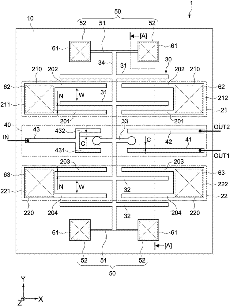
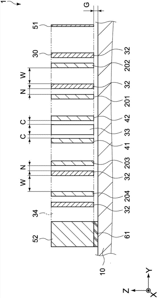
[0057] figure 1 is a schematic plan view showing the configuration of the switchgear according to the first embodiment. figure 2 is along figure 1 The cross-sectional view taken along the line [A]-[A] in. In each drawing, the X-axis and Y-axis represent plane directions orthogonal to each other, and the Z-axis represents a height (thickness) direction orthogonal to the X-axis and Y-axis. The same applies to the subsequent figures.
[0058] [Overall structure of the switchgear]
[0059] The switch device 1 according to the present embodiment is configured as a bulk silicon MEMS type electrostatically driven push / pull switch. The switching device 1 is generally produced by performing fine processing on the surface of an SOI (Silicon On Insulator) substrate. The SOI substrate includes a laminate of layers: a support layer composed of silicon, formed on the support layer and made of silicon oxide (SiO 2 ) composed of a BOX (Buried Oxide) layer, and an active layer (active l...
no. 2 approach
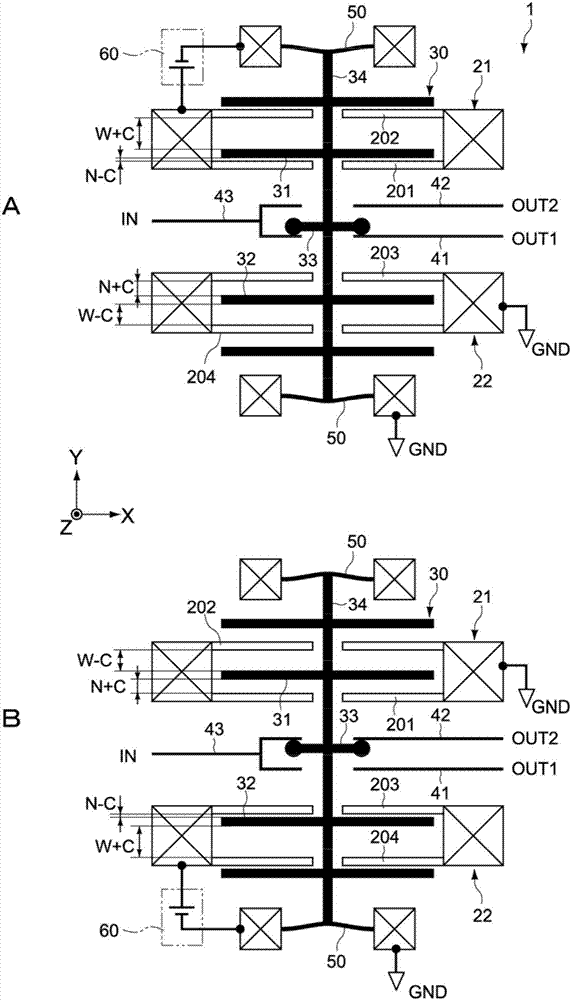
[0123] Figure 6 is a schematic plan view showing the configuration of a switchgear according to a second embodiment of the present technology. Hereinafter, configurations different from those according to the first embodiment will be mainly described, configurations that are the same as those according to the above-described embodiment will be denoted by the same reference numerals, and descriptions thereof will be omitted or simplified.
[0124] The switch device 2 according to the present embodiment is different from the switch device in the first embodiment in that movable contact points 331 and 332 are respectively provided at both ends of the connecting rod 34 of the movable electrode 30, and at the first movable An elastic support portion 50 is provided between the movable electrode piece 31 and the second movable electrode piece 32 . Since other configurations of the movable electrode 30 and configurations of the first and second fixed electrodes 21 and 22 are the sam...
no. 3 approach
[0127] Figure 7 is a schematic plan view showing the configuration of a switchgear according to a third embodiment of the present technology. Hereinafter, configurations different from those according to the first embodiment will be mainly described, configurations that are the same as those according to the above-described embodiment will be denoted by the same reference numerals, and descriptions thereof will be omitted or simplified.
[0128] The switch device 3 according to the present embodiment includes a first switch mechanism 71 and a second switch mechanism 72 . The first switch mechanism 71 and the second switch mechanism 72 are arranged to face each other in the Y-axis direction. The first switch mechanism 71 and the second switch mechanism 72 each include the same configuration as the switch device 1 described in the first embodiment.
[0129] Note that the switch mechanisms 71 and 72 are not limited thereto, and each of the switch mechanisms 71 and 72 may be co...
PUM
 Abstract
Description
Claims
Application Information
 - R&D Engineer
- R&D Manager
- IP Professional
- Industry Leading Data Capabilities
- Powerful AI technology
- Patent DNA Extraction
Browse by: Latest US Patents, China's latest patents, Technical Efficacy Thesaurus, Application Domain, Technology Topic, Popular Technical Reports.
© 2024 PatSnap. All rights reserved.Legal|Privacy policy|Modern Slavery Act Transparency Statement|Sitemap|About US| Contact US: help@patsnap.com