

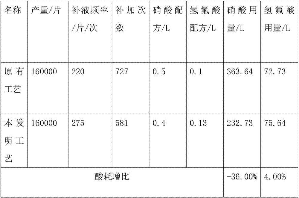
Etching process of solar energy cell chips capable of reducing NOx emissions
A solar cell and process technology, applied in sustainable manufacturing/processing, circuits, photovoltaic power generation, etc., can solve the problems of NOx pollution caused by etching nitric acid products, negative impact on the appearance and efficiency of silicon wafers, and high processing costs of NOx products. Reduce the cost of NOx treatment, reduce the amount used, and protect the environment
- Summary
- Abstract
- Description
- Claims
- Application Information
AI Technical Summary
Problems solved by technology
Method used
Image

Examples
Embodiment
[0023] The invention provides a technical solution:
[0024] A solar cell etching process that can reduce NOx emissions, comprising the following steps:
[0025] Step 1: Evenly attach deionized water to the upper surface of the silicon wafer to be etched to form a water film;
[0026] Evenly attach deionized water to the upper surface of the silicon wafer to be etched, and then let it stand for 30 seconds to form a layer of deionized water film on the upper surface, and the water film should completely and uniformly cover the silicon wafer to be etched On the upper surface, there must be no uncovered corners and water breakage to prevent the water film from breaking suddenly during etching.
[0027] Step 2: Adjust the flatness of the rollers in the etching tank to keep all the rollers in the etching tank absolutely level;
[0028] Adjust the etching tank of the etching machine in advance, and adjust the rollers used for support and conduction to keep the rollers absolutely l...
PUM
 Abstract
Description
Claims
Application Information