Method of achieving switching of PCIE bus and circuit

A bus switching and bus technology, applied in the direction of electrical digital data processing, instruments, etc., can solve the problems of increasing chip manufacturing costs, signal loss, signal integrity problems, etc., and achieve the effect of reducing signal loss

Inactive Publication Date: 2017-08-29
ZHENGZHOU YUNHAI INFORMATION TECH CO LTD
View PDF3 Cites 6 Cited by
  • Summary
  • Abstract
  • Description
  • Claims
  • Application Information

AI Technical Summary

Problems solved by technology

[0004] The switching process implemented by switching chips will bring signal integrity problems and a certain signal loss; for example, the loss at 4 GHz (GHz) is about -2 decibels (dB), which is equivalent to an intermediate printed circuit board (PCB) ) plate, about 3 inches (INCH) transmission line length, and increases the manufacturing cost of the chip

Method used


Image

  • Method of achieving switching of PCIE bus and circuit
  • Method of achieving switching of PCIE bus and circuit
  • Method of achieving switching of PCIE bus and circuit

Examples


Embodiment Construction

[0032] In order to make the purpose, technical solution and advantages of the present invention more clear, the embodiments of the present invention will be described in detail below in conjunction with the accompanying drawings. It should be noted that, in the case of no conflict, the embodiments in the present application and the features in the embodiments can be combined arbitrarily with each other.

[0033] The steps shown in the flowcharts of the figures may be performed in a computer system, such as a set of computer-executable instructions. Also, although a logical order is shown in the flowcharts, in some cases the steps shown or described may be performed in an order different from that shown or described herein.

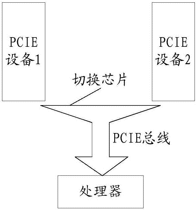
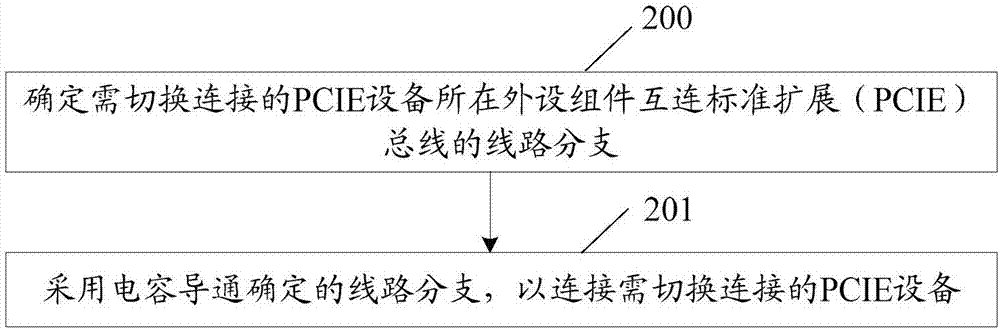
[0034] figure 2 A flow chart of a method for implementing a peripheral component interconnect standard extension (PCIE) bus switch for an embodiment of the present invention, such as figure 2 shown, including:

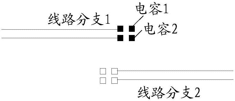
[0035] Step 200, determine the line bra...


PUM


Abstract

The invention provides a method of achieving the switching of the standard peripheral component interconnect extended (PCIE) bus and a device. The method comprises the steps that the branch circuits of PCIE bus of the PCIE devices in need of switching and connections are determined; by the branch circuits determined utilizing the breakover of capacitors, the PCIE devices in need of switching and connections are connected. By the method of achieving the switching of PCIE bus and the circuit, the breakover of the branch circuits of the PCIE devices is achieved by capacitors, the signal loss of the PCIE bus is reduced.

Description

technical field [0001] This article relates to but not limited to computer technology, especially a circuit for implementing peripheral component interconnect standard extension (PCIE) bus switching. Background technique [0002] Server systems often need to use Peripheral Component Interconnect Express (PCIE, Peripheral Component Interconnect Express) devices as external interface devices; server manufacturers expand more PCIE interfaces to be more competitive in the server market. [0003] For server systems, the number of expansion PCIE interfaces for each platform is limited. If you want to have more or more flexible PCIE configurations, it is generally achieved by adding a switching chip. figure 1 It is a schematic circuit diagram for realizing PCIE bus switching in the related art, figure 1 Taking a group of X8 PCIE buses as an example, a switching chip is used at the branch connecting two PCIE devices to perform one-to-two switching of the PCIE bus, and the switchin...

Claims


Application Information

Patent Timeline
Patent Type & Authority Applications(China)
IPC IPC(8): G06F13/40
CPCG06F13/4022
Inventor 王素华
Owner ZHENGZHOU YUNHAI INFORMATION TECH CO LTD
Why Eureka
Try Eureka