Preparation method for grid of RFLDMOS (radio frequency laterally diffused metal oxide semiconductor) device

A gate and device technology, applied in the field of gate preparation, can solve the problems of current loss, increase in loss amplitude, difficulty in mass production of high-speed and high-frequency devices, etc., and achieve the effect of reducing signal loss and increasing operating frequency

Active Publication Date: 2012-04-04
SHANGHAI HUAHONG GRACE SEMICON MFG CORP
View PDF3 Cites 3 Cited by
  • Summary
  • Abstract
  • Description
  • Claims
  • Application Information

AI Technical Summary

Problems solved by technology

However, for ordinary semiconductor factories and traditional processes, it is almost impossible to use these metals for production due to the configuration of the production line, and its output is also greatly limited.
Therefore, polysilicon resistors in most factories cannot be made to a very small level, so it is difficult to mass-produce silicon-based high-speed and high-frequency devices
[0013] When RFLDMOS works at high frequency, the high-frequency current on the gate is collected at the drain. During this process, because the frequency is extremely high, its electromagnetic field will radiate to the environment and cause current loss, and the magnitude of the loss increases with the increase of frequency. High, this effect will also restrict high-frequency applications

Method used


Image

  • Preparation method for grid of RFLDMOS (radio frequency laterally diffused metal oxide semiconductor) device
  • Preparation method for grid of RFLDMOS (radio frequency laterally diffused metal oxide semiconductor) device
  • Preparation method for grid of RFLDMOS (radio frequency laterally diffused metal oxide semiconductor) device

Examples


Embodiment Construction

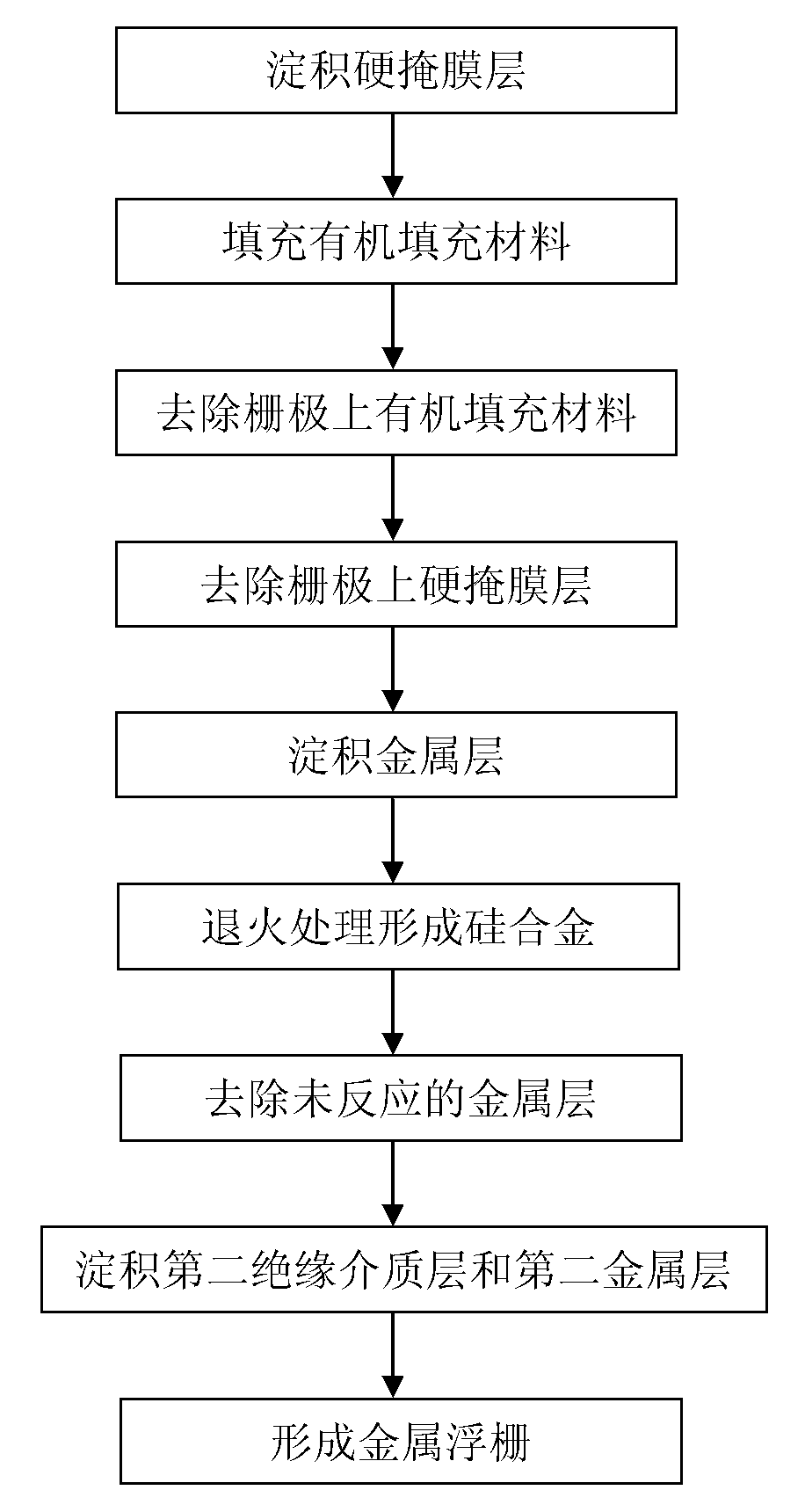
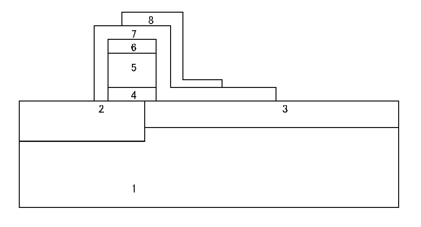
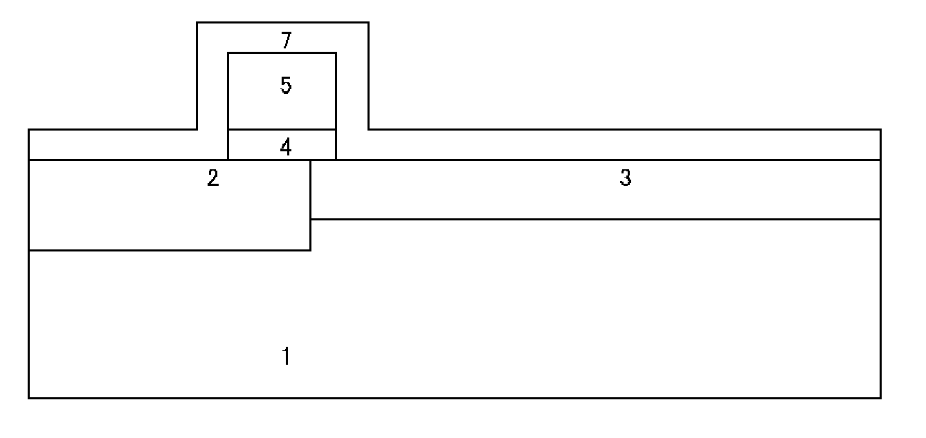
[0029] The preparation method of gate in the RFLDMOS device of the present invention, after preparing and forming source region 3, drain region 2 and polysilicon gate 5 (4 is gate oxide) on silicon chip 1, comprises the following steps (see figure 1 ):

[0030] 1) Deposit an insulating dielectric layer 7 on the silicon wafer as a hard mask layer (see image 3 );

[0031] 2) After that, fill photoresist or organic filling material on the silicon wafer to form filling layer 9 (see Figure 4 );

[0032] 3) Remove the filling layer above the gate to expose the hard mask layer on the polysilicon gate (see Figure 5 );

[0033] 4) Dry etching to remove the hard mask layer on the polysilicon gate (see Image 6 ), and then remove the remaining filling layer;

[0034] 5) depositing a metal layer 10 alloyed with silicon (see Figure 7 );

[0035] 6) Annealing is used to make the metal of the metal layer and the polysilicon form a silicon alloy 6 (see Figure 8 );

[0036] 7) r...


PUM

PropertyMeasurementUnit
thicknessaaaaaaaaaa
thicknessaaaaaaaaaa
thicknessaaaaaaaaaa

Abstract

The invention discloses a preparation method for a grid of a RFLDMOS (radio frequency laterally diffused metal oxide semiconductor) device. A metal floating grid structure wrapping a grid and a drain is further prepared during preparation of a low-resistance metal grid, and is capable of effectively shielding high-frequency signals.

Description

technical field [0001] The invention relates to a preparation method of a gate in an RFLDMOS device. Background technique [0002] Semiconductor devices based on polysilicon gates are currently mainstream semiconductor devices, and are widely manufactured and used. However, due to the material itself, since the silicon material itself is a semiconductor material rather than a conductor material, its resistivity is relatively high. Although doping can be used to reduce its resistivity, it has its limit. The typical implantation doping process can only reach a bulk concentration of 10 21 ~10 22 atom / cm3 (atoms per cubic centimeter), its resistivity is about 40-100 ohms / cm. Therefore, for high-speed devices, their resistivity greatly restricts the improvement of speed and frequency. In order to reduce the resistivity of the device gate, a common method is to form polysilicon into a metal silicide, and the commonly used metal silicide is SiW. However, the resistivity of a t...

Claims


Application Information

Patent Timeline
Patent Type & Authority Applications(China)
IPC IPC(8): H01L21/28
Inventor 王雷王海军
Owner SHANGHAI HUAHONG GRACE SEMICON MFG CORP
Why Eureka
Try Eureka