Substrate with cooler for power modules and method for producing same

A technology of power module and manufacturing method, applied in semiconductor/solid-state device manufacturing, manufacturing tools, printed circuit manufacturing, etc., can solve problems such as deformation of aluminum coolers, and achieve the effect of high bonding reliability and low thermal resistance

Inactive Publication Date: 2017-08-29
MITSUBISHI MATERIALS CORP
View PDF4 Cites 5 Cited by
  • Summary
  • Abstract
  • Description
  • Claims
  • Application Information

AI Technical Summary

Problems solved by technology

[0008] However, the brazing process is performed by pressurizing and heating the metal plates laminated via the brazing material in the lamination direction. Therefore, the aluminum-made

Method used


Image

  • Substrate with cooler for power modules and method for producing same
  • Substrate with cooler for power modules and method for producing same
  • Substrate with cooler for power modules and method for producing same

Examples


no. 1 Embodiment approach

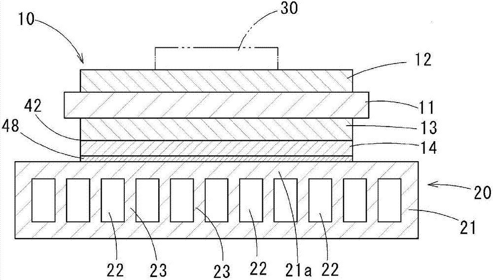
[0038] figure 1 The shown power module substrate 10 with a cooler has: a ceramic substrate 11; a circuit layer 12 bonded to one surface of the ceramic substrate 11; a first metal layer 13 bonded to the other surface of the ceramic substrate 11; The metal layer 14 is bonded to the surface of the first metal layer 13 opposite to the ceramic substrate 11; the cooler 20 is bonded to the second metal layer 14; and the titanium layer 42 is interposed between the first metal layer 13 and the second metal layer 14. figure 1 Indicated at 48 is an adhesive layer which will be described later. And, if figure 1 As shown by the two-dot chain line in , the semiconductor element 30 is bonded on the circuit layer 12 with a solder material to form a power module.

[0039] The ceramic substrate 11 prevents electrical connection between the circuit layer 12 and the first metal layer 13, and it can use aluminum nitride (AlN), silicon nitride (Si 3 N 4 ), alumina (Al2 o 3 ), etc., but among ...

no. 2 Embodiment approach

[0075] Such as Figure 4 As shown, the power module substrate 210 with a cooler according to the second embodiment of the present invention includes: a ceramic substrate 211; a circuit layer 212 bonded to one surface of the ceramic substrate 211 and made of copper or a copper alloy; The metal layer 213 is bonded to the other surface of the ceramic substrate 211 and is made of copper or a copper alloy; the second metal layer 214 is bonded to the first metal layer 213 and is made of nickel or a nickel alloy; and the cooler 20 is bonded to the first metal layer 213. 2. The metal layer 214 is made of aluminum alloy. In addition, as in the first embodiment, part of the double cladding material for brazing the cooler 20 remains between the second metal layer 214 and the cooler 20 as the joining layer 48 .

[0076] In this power module substrate 210 with a cooler, Ni in the second metal layer 214 bonded to the surface of the first metal layer 213 exists in a diffused state, and in t...

no. 3 Embodiment approach

[0080] Such as Figure 5 As shown, the power module substrate 310 with a cooler according to the third embodiment of the present invention includes: a ceramic substrate 311; a circuit layer 312 bonded to one surface of the ceramic substrate 311 and made of copper or a copper alloy; The metal layer 313 is bonded to the other surface of the ceramic substrate 311 and is made of copper or a copper alloy; the second metal layer 314 is bonded to the first metal layer 313 and is made of nickel or a nickel alloy; and the cooler 20 is bonded to the first metal layer 313. The second metal layer 314 is made of aluminum alloy, and also has an aluminum layer 315 interposed between the second metal layer 314 and the cooler 20 . In addition, a part of the double-clad material used to braze and join the cooler 20 remains between the aluminum layer 315 and the cooler 20 as the joining layer 48 similarly to each of the above-described embodiments.

[0081] In this power module substrate 310 wi...


PUM

PropertyMeasurementUnit
Thicknessaaaaaaaaaa
Thicknessaaaaaaaaaa
Thicknessaaaaaaaaaa

Abstract

Provided is a substrate with a cooler for power modules, which is prevented from the occurrence of deformation during brazing of a metal layer that is formed from copper or a copper alloy to a cooler that is formed from aluminum, and which has low thermal resistance and high bonding reliability. A circuit layer that is formed from copper or a copper alloy is bonded to one surface of a ceramic substrate, while bonding a metal layer that is formed from copper or a copper alloy to the other surface of the ceramic substrate. A second metal layer that is formed from aluminum or an aluminum alloy is bonded to the metal layer by solid-phase diffusion, and a cooler that is formed form an aluminum alloy is joined to the second metal layer by brazing with use of an Mg-containing Al-based brazing filler material.

Description

technical field [0001] The present invention relates to a substrate for a power module with a cooler used in controlling a large current and a high voltage semiconductor device and a manufacturing method thereof. [0002] This application claims priority based on Patent Application No. 2014-211529 filed on October 16, 2014 and Patent Application No. 2015-200784 filed on October 9, 2015, and the contents thereof are incorporated herein. Background technique [0003] As a conventional power module substrate, there is known a structure in which a circuit layer is bonded to one surface of a ceramic substrate serving as an insulating layer, and a metal layer for heat dissipation is bonded to the other surface. In addition, a cooler is bonded to the metal layer of the power module substrate to constitute a power module substrate with a cooler. Furthermore, a semiconductor element such as a power element is mounted on the circuit layer via a solder material to form a power module....

Claims


Application Information

Patent Timeline
IPC IPC(8): H01L23/36H01L23/12
CPCH01L2924/0002H01L23/3735H01L23/473C04B37/026C04B2237/125C04B2237/127C04B2237/343C04B2237/366C04B2237/368C04B2237/407C04B2237/704C04B2237/706H01L23/3736H01L2924/00H01L23/12H01L23/3731B23K20/02H01L21/4882H05K1/0203H05K3/20
Inventor 大井宗太郎大开智哉北原丈嗣
Owner MITSUBISHI MATERIALS CORP
Why Eureka
Try Eureka