Magnetic nanowire device, manufacturing method thereof and magnetic nanowire construction method

A technology of magnetic nanometers and manufacturing methods, which is applied in the field of memory and can solve problems such as the inability to provide magnetic nanowires

Active Publication Date: 2017-09-01
INST OF MICROELECTRONICS CHINESE ACAD OF SCI
View PDF1 Cites 2 Cited by
  • Summary
  • Abstract
  • Description
  • Claims
  • Application Information

AI Technical Summary

Problems solved by technology

[0006] The main purpose of this application is to provide a magnetic nanowire device, its manufacturing method and a method for constructing magnetic nanowires, so as to solve the problem that a confined and stable magnetic nanowire cannot be provided in the prior art

Method used


Image

  • Magnetic nanowire device, manufacturing method thereof and magnetic nanowire construction method
  • Magnetic nanowire device, manufacturing method thereof and magnetic nanowire construction method
  • Magnetic nanowire device, manufacturing method thereof and magnetic nanowire construction method

Examples


Embodiment

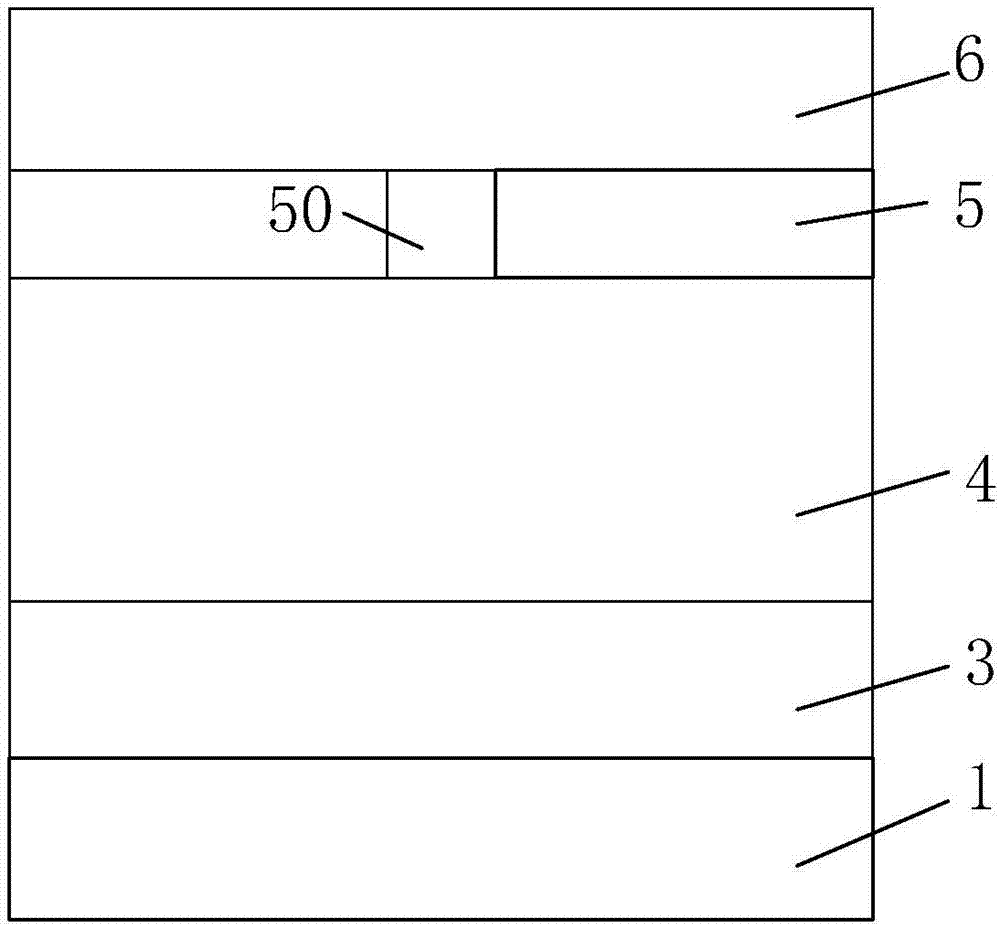
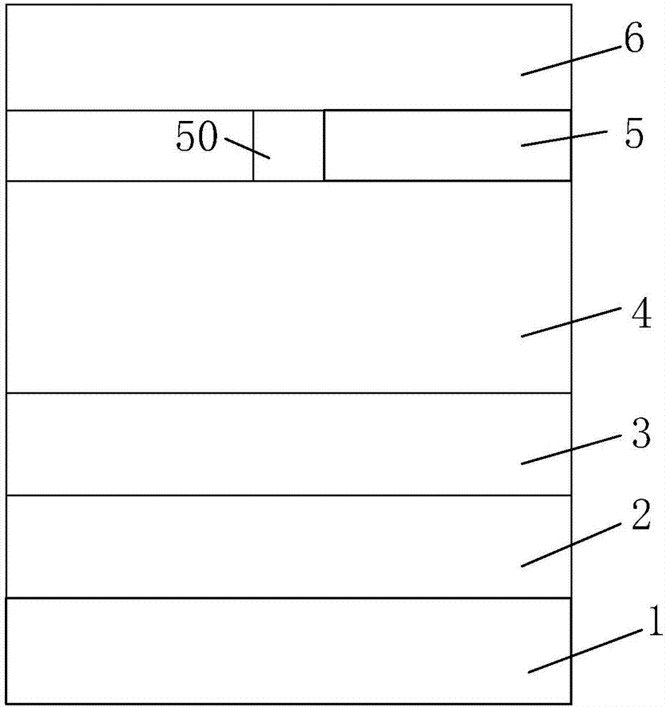
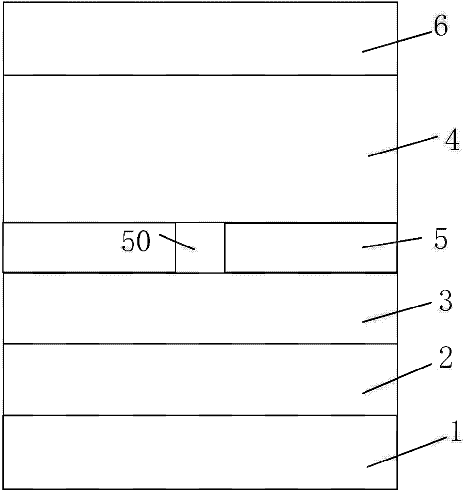
[0103] The construction process of magnetic nanowires is as follows:

[0104] First, a magnetic nanowire device is formed.

[0105] Electron beam evaporation on insulating substrate SiO 2 Deposit a layer of Ti metal film on the Ti metal film with a thickness of 10nm to form a seed layer; then, use electron beam evaporation to deposit a Pt electrode layer on the Ti metal film with a thickness of 30nm to form the first electrode layer; use magnetron sputtering Deposit a layer of 20nm thick HfO on the Pt electrode layer by radiation method 2 insulating layer; followed by HfO 2 Transfer single-layer graphene with nanopores on the insulating layer as the atomic barrier layer; then use electron beam evaporation to deposit 50nm Fe on the atomic barrier layer as the second electrode layer to form a magnetic nanowire device.

[0106] Second, the formation of magnetic nanowires

[0107] Apply positive scan voltages at equal intervals to the ferromagnetic electrode layer, and the non...


PUM

PropertyMeasurementUnit
thicknessaaaaaaaaaa
thicknessaaaaaaaaaa
thicknessaaaaaaaaaa

Abstract

The invention provides a magnetic nanowire device, a manufacturing method thereof and a magnetic nanowire construction method. The magnetic nanowire device comprises a substrate, a first electrode layer, an insulating layer, an atomic barrier layer and a second electrode layer sequentially arranged in a stacked mode, wherein one of the first electrode layer and the second electrode layer serves as a ferromagnetic electrode layer, and the other is a non-magentic electrode layer. The magnetic nanowire device also comprises the atomic barrier layer arranged between the ferromagnetic electrode layer and the insulating layer; and the atomic barrier layer comprises a nano through hole. The magnetic nanowire device can effectively and accurately control the width and the position of a magnetic nanowire, and confinement and stabilization of the nanowire can be realized. The magnetic nanowire device realizes magnetoelectric coupling effects, and a carrier is provided for studying a new multilevel memory device.

Description

technical field [0001] The present application relates to the field of memory, and in particular, relates to a magnetic nanowire device, a manufacturing method thereof, and a construction method of the magnetic nanowire. Background technique [0002] In recent years, people have developed many new information materials and devices. Such as flash memory, resistive memory (RRAM), magnetic recording, magnetic memory (MRAM), etc., among these technologies, some use the charge property of electrons, and some use the spin property of electrons. [0003] MRAM utilizes the spin properties of electrons. Its basic structure is a spin valve or magnetic tunnel junction (two ferromagnetic layers are separated by a non-magnetic metal layer or insulating layer), and it works based on the magnetoresistance effect. Among them, a ferromagnetic layer The magnetization direction of the ferromagnetic layer is fixed and the magnetization direction of the other ferromagnetic layer changes with th...

Claims


Application Information

Patent Timeline
Patent Type & Authority Applications(China)
IPC IPC(8): H01L43/08H01L43/02H01L43/12B82Y40/00B82Y10/00B82Y25/00H10N50/10H10N50/01H10N50/80
CPCB82Y10/00B82Y25/00B82Y40/00H10N50/80H10N50/10H10N50/01
Inventor 龙世兵李磊磊滕蛟刘琦吕杭炳刘明
Owner INST OF MICROELECTRONICS CHINESE ACAD OF SCI
Why Eureka
Try Eureka