
Wafer level chip scale package (WLCSP) structure with through-silicon via continuous state and manufacturing method thereof

A technology of size packaging and TSV, applied in semiconductor/solid-state device manufacturing, semiconductor/solid-state device components, electrical components, etc., to reduce wafer size, save costs, and avoid cracking and damage

Active Publication Date: 2017-09-12
POWERTECH TECHNOLOGY INC
View PDF6 Cites 0 Cited by
  • Summary
  • Abstract
  • Description
  • Claims
  • Application Information

AI Technical Summary

Problems solved by technology

[0004] In order to solve the above-mentioned technical problems, the main purpose of the present invention is to provide a wafer-level chip-scale packaging structure with a continuous type of TSV and a manufacturing method thereof, so as to achieve a continuous type of TSV in a composite wafer structure without any Process contamination caused by hole over-etching and electrical connection failure in the hole

Method used


Image

  • Wafer level chip scale package (WLCSP) structure with through-silicon via continuous state and manufacturing method thereof
  • Wafer level chip scale package (WLCSP) structure with through-silicon via continuous state and manufacturing method thereof
  • Wafer level chip scale package (WLCSP) structure with through-silicon via continuous state and manufacturing method thereof

Examples


no. 1 Embodiment

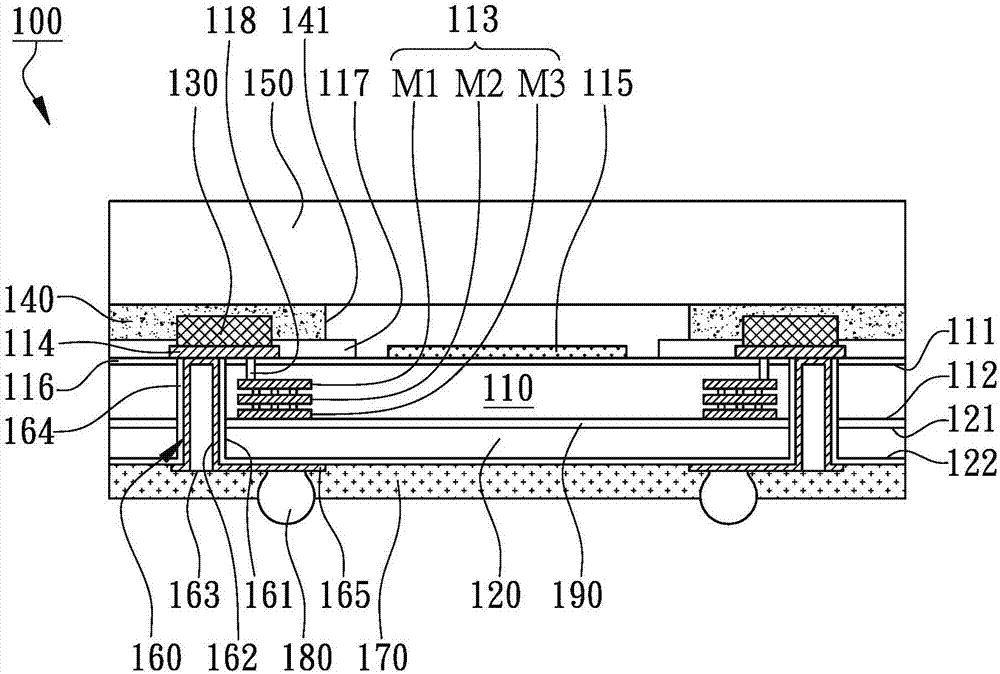
[0064] According to the first embodiment of the present invention, a TSV continuous wafer-level chip-scale packaging structure 100 is illustrated in figure 1 cross-sectional schematic diagram. The WLCSP structure 100 includes a device chip 110, a carrier chip 120, at least one spacer conductor bump 130, a spacer adhesive layer 140, a protective cover sheet 150, at least one TSV structure 160, and a protective layer. 170 and a plurality of external terminals 180.

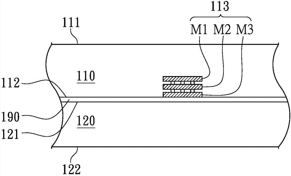
[0065] see figure 1 , the main body of the device chip 110 has a first surface 111 and a second surface 112; usually the main body of the device chip 110 is a semiconductor material layer, such as monocrystalline silicon, on the first surface 111 of the device chip 110 can be An insulating layer 116 is formed. A metal interconnect parallel pad assembly 113 is embedded in the device wafer 110, at least one offset pad 114 is disposed on the first surface 111 and connected to the metal interconnect parallel pad assem...

no. 2 Embodiment

[0085] According to the second embodiment of the present invention, another WLCSP structure 200 with TSV continuous type is described in image 3 A cross-sectional schematic diagram of , wherein the components corresponding to the same names and functions of the first specific embodiment are represented by the same component figure numbers of the first specific embodiment, and the same detailed features will not be repeated. The WLCSP structure 200 includes a device chip 110, a carrier chip 120, at least one spacer conductor bump 230, a spacer adhesive layer 140, a protective cover sheet 150, at least one TSV structure 160, and a protective layer. 170 and a plurality of external terminals 180.

[0086] see image 3 The main body of the device chip 110 has a first surface 111 and a second surface 112 , wherein a metal interconnect parallel pad assembly 113 is embedded in the device chip 110 . At least one offset pad 114 is disposed on the first surface 111 and connected to th...


PUM


Abstract

The invention discloses a wafer level chip scale package (WLCSP) structure with a through-silicon via continuous state and a manufacturing method thereof. The WLCSP structure mainly comprises a device chip, a carrier chip laminated on the device chip, a protective cover, and a through-silicon via structure. A metal interlinked parallel pad combination is embedded in the device chip. An offset pad is arranged on the device chip and is connected to the metal interlinked parallel pad combination. A partition conductor lug is arranged on the offset pad. A partition adhesive layer is formed on the device chip and covers the partition conductor lug. The protective cover is pressed on the partition adhesive layer. The through-silicon via structure comprises a through hole and a porous metal layer. The through hole is slightly-eccentrically aligned to the offset pad and penetrates the carrier chip and the device chip continuously. The porous metal layer is formed in the through hole and is connected to the offset pad. The through hole is non-centrally aligned to the partition conductor lug. A protective layer is formed on the carrier chip and covers the through hole. The conductor lug is partitioned by the offset pad so as to ensure the continuous state of the through-silicon via structure.

Description

technical field [0001] The present invention relates to the field of semiconductor chip packaging, in particular to a wafer-level chip size packaging structure with continuous through-silicon vias and a manufacturing method thereof, which is applicable to the packaging application of CMOS image sensor chips. Background technique [0002] Wafer Level Chip Scale Package (WLCSP) is different from the traditional chip packaging method. It is packaged and tested on the entire wafer first, and then cut into individual package structures containing IC particles. And the size of the semiconductor package is not larger than the area of ​​1.44 times of the chip size, effectively reducing the volume of the semiconductor package. Generally, the WLCSP structure has a double-sided vertical electrical connection structure for bonding external terminals to the bottom of the chip, so as to reduce the size of the substrate or omit the substrate components. The existing double-sided vertical ...

Claims


Application Information

Patent Timeline
Patent Type & Authority Applications(China)
IPC IPC(8): H01L23/31H01L23/498H01L21/56
CPCH01L21/561H01L23/3107H01L23/3128H01L23/49816H01L23/49827H01L23/49838H01L21/76898H01L23/3114H01L27/14618H01L27/14627H01L27/14632H01L27/14636H01L21/56H01L23/3121H01L23/481H01L23/562H01L24/03H01L24/06H01L24/11H01L24/13H01L24/32H01L24/83H01L2224/0237H01L2224/0401H01L2224/05124H01L2224/05147H01L2224/1134H01L2224/11462H01L2224/13016H01L2224/13027H01L2224/13139H01L2224/13144H01L2224/13147H01L2224/13155H01L2224/32225H01L2224/73253H01L2924/0132H01L2924/15311
Inventor 方立志张家彰徐宏欣张文雄鍾基伟连加雯
Owner POWERTECH TECHNOLOGY INC
Features
  • Generate Ideas
  • Intellectual Property
  • Life Sciences
  • Materials
  • Tech Scout
  • Unparalleled Data Quality
  • Higher Quality Content
  • 60% Fewer Hallucinations
Learn More