Automatic wedge bonding method on micro bonding pad in overlaying or side-by-side manner

An automatic, wedge welding technology, applied in the field of microelectronics, can solve problems such as breakage, lead wire contact deformation, etc., to achieve the effect of reducing size, reducing quantity and improving coverage

Active Publication Date: 2017-09-15
SOUTHWEST CHINA RES INST OF ELECTRONICS EQUIP
View PDF5 Cites 6 Cited by
  • Summary
  • Abstract
  • Description
  • Claims
  • Application Information

AI Technical Summary

Problems solved by technology

When using an automatic wedge welding machine for welding, because the fixture fixes the parts to be welded, the chopper and the welded leads will interfere with each other when welding multiple leads on the micro-pad, so there is a common occurrence in the process of bonding the latter lead. The phenomenon that the previous bonded lead wire is touched and deformed, or even broken

Method used


Image

  • Automatic wedge bonding method on micro bonding pad in overlaying or side-by-side manner
  • Automatic wedge bonding method on micro bonding pad in overlaying or side-by-side manner
  • Automatic wedge bonding method on micro bonding pad in overlaying or side-by-side manner

Examples


example 1

[0051] In this example 1, the improved wedge knife is used to perform overlapping wedge bonding on the micro-pad, so as to realize superposition bonding of 2 leads on the micro-pad by using an automatic wedge bonder.

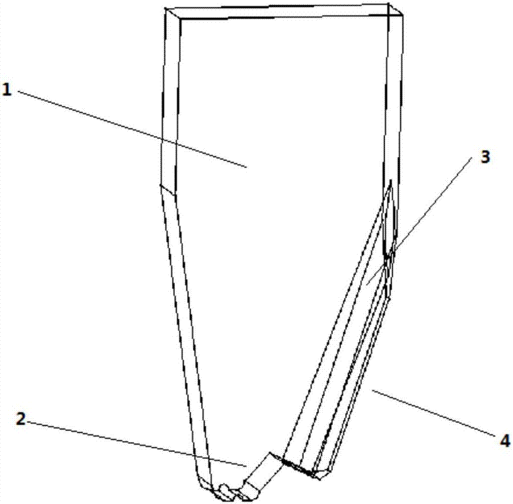
[0052] The structural schematic diagram of the improved automatic wedge-bonded hacking knife in Example 1 is as follows: figure 1 shown. It includes a rivet main body 1, a rivet end 2 and a thread hole 3, the rivet end 2 is located at the end of the rivier main body 1, the thread hole 3 runs through the rivier main body 1 and forms an angle with the side of the main body, A notch 4 is formed on the side of the riving knife end 2 .

[0053] In this example 1, the improved automatic wedge-bonded rivet is used, and a notch 4 is formed on the side of the end 2 of the rivet, which can effectively prevent the end 2 of the rivet from deforming or even breaking the bonded leads. The schematic diagram of the interference of two wires superimposed and bonded by using an...

example 2

[0059] In this example 2, an improved rivet is used to perform side-by-side wedge bonding on the micro-pad, so that two wires can be bonded side by side on the micro-pad by using an automatic wedge bonder.

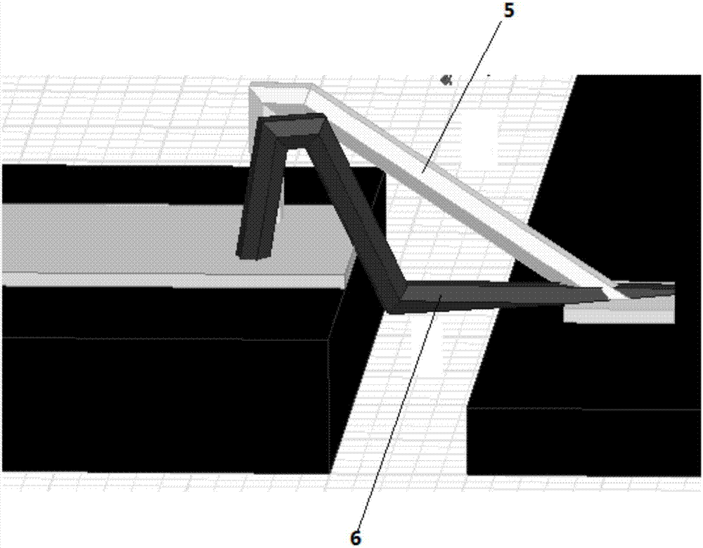
[0060] Figure 5 The top view of the side-by-side bonding structure of the micro-pads with two leads that are obtained by side-by-side bonding on the semiconductor chip 8 micro-pads by adopting the improved chopper for example 2; Figure 5 As shown, in this example 2, the specific process of bonding two wires side by side on the 8 micro-pads of the semiconductor chip is as follows:

[0061] Adopting the improved automatic wedge-bonding hacker, on the pad of the substrate circuit sheet 7, adopting common bonding mode, bonding the first bonding point of the first lead 5 to the micro-pad 9 of the substrate circuit sheet 7, That is to realize the bonding of the first lead 5 on the substrate circuit sheet 7 and the semiconductor chip 8 respectively;

[0062] Using the improve...


PUM


Abstract

The invention provides an automatic wedge bonding method on a micro bonding pad in an overlaying or side-by-side manner, and belongs to the technical field of microelectronics. According to the automatic wedge bonding method, a first bonding point of a first lead is bonded on a bonding pad of a first base material, and a second bonding point of the first lead is bonded on a micro bonding pad of a second base material; an improved automatic wedge bonding chopper is adopted, and the first bonding point of the second lead is bonded on the bonding pad of the first base material, and the second bonding point of the second lead is bonded above the second bonding point of the first lead in an overlaying manner or bonded in a position close to the second bonding point of the first lead in a side-by-side manner; and the above operation is executed repeatedly until the overlaying or side-by-side bonding of the last lead is completed. The invention provides the method for bonding at least two leads on the micro bonding pad in the overlaying or side-by-side manner by an automatic wedge bonding machine, so that the coverage rate of the bonded leads can be improved; and by combining the bonding pads with the same functions on a semiconductor chip, the number of input and output bonding pads can be reduced, thereby further reducing the dimension of the semiconductor chip.

Description

technical field [0001] The invention belongs to the technical field of microelectronics, and more specifically relates to a bonding method for superimposing or side by side bonding at least two wires on a micro pad by using an automatic wedge bonder. Background technique [0002] The chip pads of semiconductor devices are getting smaller and smaller, and the unilateral size of pads has been reduced from 100 microns to 30 microns and below. In addition, in the field of optoelectronics and the interconnection of semiconductor devices in high-frequency components such as millimeter waves and microwaves, due Multiple leads reduce parasitic inductance and other factors compared with a single lead, and at least 2 leads must be bonded on the micro-pad of the input and output of the semiconductor device. At present, a manual wedge bonder is generally used to realize the simultaneous superposition bonding of a single pad or side-by-side bonding of two lead wire structures to achieve ...

Claims


Application Information

Patent Timeline
Patent Type & Authority Applications(China)
IPC IPC(8): H01L21/603H01L23/49
CPCH01L24/49H01L24/85H01L2224/49426H01L2224/85203H01L2224/49111
Inventor 罗建强王辉文泽海
Owner SOUTHWEST CHINA RES INST OF ELECTRONICS EQUIP
Why Eureka
Try Eureka