
ESD protection circuit structure of silicon-gate MOS integrated circuit

An ESD protection, integrated circuit technology, applied in circuits, electrical components, electrical solid devices, etc., can solve the problems of high electrostatic voltage and energy of chips, large secondary protection area, and high resistance requirements, and achieve good electrostatic discharge effect and protection. circuit, the effect of reducing the area

Pending Publication Date: 2017-09-15
深圳市航顺芯片技术研发有限公司
View PDF3 Cites 1 Cited by
  • Summary
  • Abstract
  • Description
  • Claims
  • Application Information

AI Technical Summary

Problems solved by technology

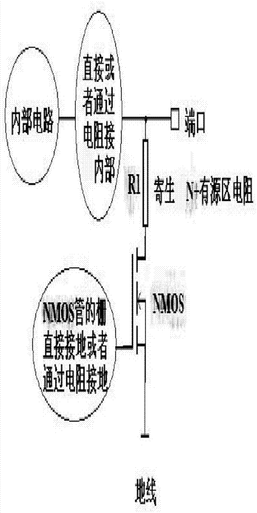
[0002] The ESD protection of traditional silicon-gate MOS integrated circuits has many circuits with simple structures, among which the gate is directly grounded or the gate is grounded through a resistor. It is difficult for this circuit to ensure that the port first passes through the NMOS tube (which works The main reason is that the parasitic NPN triode) discharges static electricity, and then discharges static electricity through the resistor, which is easy to burn the resistor, or the resistance is relatively high, and the static voltage and energy reaching the chip are relatively high, and the single-stage protection effect is not good. Disadvantages of large level protection area

Method used


Image

  • ESD protection circuit structure of silicon-gate MOS integrated circuit
  • ESD protection circuit structure of silicon-gate MOS integrated circuit
  • ESD protection circuit structure of silicon-gate MOS integrated circuit

Examples


specific Embodiment

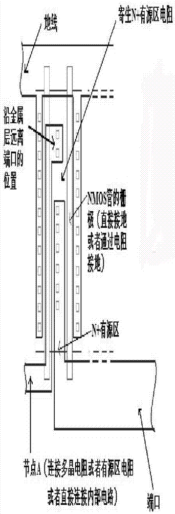
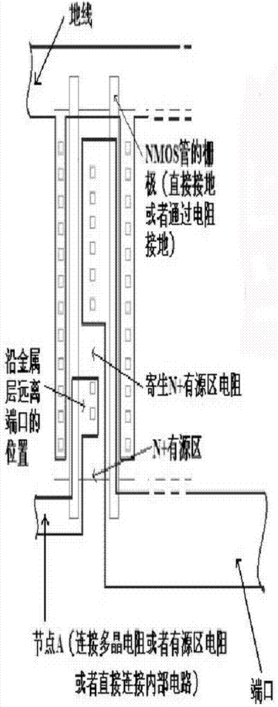
[0021] Such as figure 2 , image 3 , Figure 4 As shown, take a multi-fingered NMOS transistor with a common drain (drain connected to the port) and two NMOS transistors, along the metal layer, use the N+N type active area injection resistance parasitic in the NMOS at a position away from the port , to ensure that most of the static electricity is first discharged through the multi-fingered NMOS tube, and then directly connected to the internal circuit through the parasitic N-type active area injection resistor in the NMOS or through the polycrystalline resistor or the active area resistor.

[0022] The invention not only reduces the area of ​​the integrated circuit layout by setting the N-type active area injection resistor on the NMOS tube, but also ensures that most of the static electricity is first discharged through the NMOS tube, and then injected into the resistor through the N-type active area. Connected to the internal circuit, the electrostatic discharge effect i...


PUM


Abstract

The invention discloses an ESD protection circuit structure of a silicon-gate MOS integrated circuit. The ESD protection circuit structure comprises an NMOS (N-channel metal oxide semiconductor) transistor, an internal circuit, a port and an N-type active region injection resistor, and is characterized in that the NMOS transistor is connected with the internal circuit and the port, the NMOS transistor is provided with the N-type active region injection resistor, the N-type active region injection resistor is connected with the internal circuit and the port, and the internal circuit is connected with the port. The NMOS transistor is provided with the N-type active region injection resistor, thereby not only reducing the area of the integrated circuit layout, but also ensuring that most static electricity is firstly discharged through the NMOS transistor and then connected to the internal circuit through the N-type active region injection resistor, being good in electrostatic discharge effect, facilitating circuit protection and being low in cost.

Description

technical field [0001] The invention relates to the technical field of integrated circuit structures, in particular to a silicon gate MOS integrated circuit ESD protection circuit structure. Background technique [0002] The ESD protection of traditional silicon-gate MOS integrated circuits has many circuits with simple structures, among which the gate is directly grounded or the gate is grounded through a resistor. It is difficult for this circuit to ensure that the port first passes through the NMOS tube (which works The main reason is that the parasitic NPN triode) discharges static electricity, and then discharges static electricity through the resistor, which is easy to burn the resistor, or the resistance is relatively high, and the static voltage and energy reaching the chip are relatively high, and the single-stage protection effect is not good. The disadvantage of the level protection area is too large. The above deficiencies are worth addressing. Contents of the...

Claims


Application Information

Patent Timeline
Patent Type & Authority Applications(China)
IPC IPC(8): H01L27/02
CPCH01L27/0288
Inventor 刘吉平张怀东周蕴言冯冰
Owner 深圳市航顺芯片技术研发有限公司
Learn More