Wiring structure and wiring layout system and method of programmable logic device

A technology of programming logic and layout method, which is applied in the fields of instrumentation, computing, and electrical digital data processing, etc., and can solve the problems of reduced connectivity, increased cost, and reduced manufacturing cost, etc.

Active Publication Date: 2020-11-17
SHANGHAI ANLOGIC INFOTECH CO LTD
View PDF6 Cites 0 Cited by
  • Summary
  • Abstract
  • Description
  • Claims
  • Application Information

AI Technical Summary

Problems solved by technology

The more transmission gates introduced, the greater the connectivity of the wiring, and the difficulty of wiring is reduced. The problem caused is that the area of ​​the device will also increase, and the cost will increase.
Conversely, if there are fewer transmission gates in the design, the connectivity of the wiring will be smaller, and the difficulty of wiring will increase, but the area of ​​the device will also be smaller, and the manufacturing cost will also decrease.

Method used


Image

  • Wiring structure and wiring layout system and method of programmable logic device
  • Wiring structure and wiring layout system and method of programmable logic device
  • Wiring structure and wiring layout system and method of programmable logic device

Examples


Embodiment Construction

[0076] In the following description, many technical details are proposed in order to enable readers to better understand the application. However, those skilled in the art can understand that without these technical details and various changes and modifications based on the following implementation modes, the technical solution claimed in each claim of the present application can be realized.

[0077] In order to make the purpose, technical solution and advantages of the present invention clearer, the following will further describe the implementation of the present invention in detail in conjunction with the accompanying drawings.

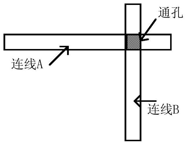
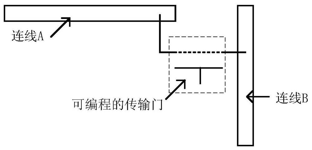
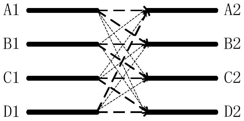
[0078] A programmable logic device (such as a Field Programmable Gate Array (FPGA) device) contains a large number of various connection resources, and these connections will be grouped and placed in preset line tracks on the chip according to certain rules. In the research of FPGA academia, there are some high-connectivity wiring structures, each...


PUM


Abstract

The invention relates to layout design and a software system of a programmable logic device, and discloses a connection structure of the programmable logic device, a wiring system and method of the programmable logic device and a layout system and method of the programmable logic device. In the connection structure of the programmable logic device, only adjacent wire rails in one wire rail group are connected through a programmable transmission gate, so that a cross-wire rail group programmable transmission gate is saved; new multipath selectors are increased to serve as wire rail selectors, so that wire rails of different wire rail groups can be accessed to logic units, the connectivity of all the wire rails is provided, and then the chip area, power consumption and construction cost are decreased while the connectivity of each wire rail group is kept. Moreover, the layout and wiring of the programmable logic device are improved, so that the routing rate of the connection structure is further improved and the using quantity of the multipath selectors is decreased.

Description

technical field [0001] The invention relates to a programmable logic device layout design and software system, in particular to a wiring structure and wiring layout system and method of a programmable logic device. Background technique [0002] An ASIC is an integrated circuit customized by the user to realize a specific function, in which all integrated circuit devices and device connections are not preset, and can be arranged according to actual circuit needs. However, once the connection and function are designed, they cannot be changed. A programmable logic device is an integrated circuit in which the devices and wiring resources in the chip have been pre-arranged, but the device functions can be reconfigured through programming. The production of all integrated circuit chips (including programmable logic devices) relies on the processing of wafers and metal layers by photolithography. Different chips have an independent series of photolithography masks (Mask). Layout...

Claims


Application Information

Patent Timeline
Patent Type & Authority Patents(China)
IPC IPC(8): G06F30/347
CPCG06F30/34G06F30/392
Inventor 文化董辰谢丁王元黄志军
Owner SHANGHAI ANLOGIC INFOTECH CO LTD
Why Eureka
Try Eureka