
Thin film transistor array substrate and preparation method thereof

A technology of thin film transistors and array substrates, which is applied in the field of liquid crystal display preparation, and can solve problems such as increased product defects, increased contact resistance, and metal corrosion

Active Publication Date: 2017-09-22
SHENZHEN CHINA STAR OPTOELECTRONICS SEMICON DISPLAY TECH CO LTD
View PDF6 Cites 1 Cited by
  • Summary
  • Abstract
  • Description
  • Claims
  • Application Information

AI Technical Summary

Problems solved by technology

[0004] The disadvantage of the existing lift-off process is that the normal via hole design is adopted in the lift-off process, and the transparent conductive film (ITO) cannot completely cover the via hole, such as Figure 1C As shown, the metal part of the drain at the electrical connection of the via hole is exposed, which may cause metal corrosion in the subsequent process, resulting in an increase in contact resistance, forming dark spots or dark lines, increasing product defects, and reducing product quality and reliability.

Method used


Image

  • Thin film transistor array substrate and preparation method thereof
  • Thin film transistor array substrate and preparation method thereof
  • Thin film transistor array substrate and preparation method thereof

Examples


Embodiment Construction

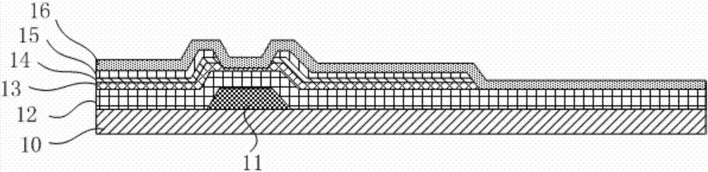
[0018] The specific embodiments of the thin film transistor array substrate and the preparation method thereof provided by the present invention will be described in detail below with reference to the accompanying drawings.

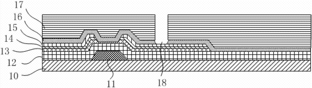
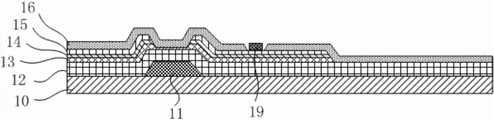
[0019] The present invention provides a method for preparing a thin film transistor array substrate, see figure 2 , the method includes the following steps: step S200 , providing a base substrate, and sequentially forming a gate electrode, a gate insulating layer, an active layer, an ohmic contact layer, a source / drain electrode and an insulating layer on the base substrate; step S201 , coating a photoresist layer on the insulating layer; step S202, exposing the photoresist layer, patterning the photoresist layer, exposing the insulating layer at the corresponding position where the pixel electrode is to be formed, and forming a distribution in the exposed The first photoresist region on the periphery of the insulating layer and the second photoresist re...


PUM


Abstract

The invention provides a thin film transistor array substrate and a preparation method thereof. The method comprises the steps that a substrate is provided; a gate, a gate insulating layer, an active layer, an ohmic contact layer, a source / drain and an insulating layer are successively formed on the substrate; a photoresist layer is coated on the insulating layer; the photoresist layer is exposed to pattern the photoresist layer; the insulating layer is exposed at a corresponding position where a pixel electrode is to be formed, and a first photoresist region distributed around the insulating layer and a second photoresist region distributed in the periphery of the first photoresist region are formed, wherein the thickness of the photoresist layer of the first photoresist region is less than the thickness of the photoresist layer of the second photoresist region; the exposed insulating layer is removed through an etching process to form a via hole and expose the drain, and the first photoresist region corresponds to the upper edge of the via hole; the photoresist layer is subjected to ashing processing to remove the first photoresist region and expose the vias sidewall, and partial second photoresist region is retained; a pixel electrode is formed in the via hole; and the pixel electrode covers the vias sidewall to form a thin film transistor array substrate.

Description

technical field [0001] The invention relates to the field of preparation of liquid crystal displays, in particular to a thin film transistor array substrate and a preparation method thereof. Background technique [0002] In the information society, flat panel displays are ubiquitous, whether it is TVs, computers, smartphones, etc., they are inseparable from the support of LCD panels. People's demand for display equipment continues to grow, which also promotes the rapid development of the liquid crystal display panel industry. The output of liquid crystal panels continues to increase, and there are higher requirements for product quality and yield. Cost saving has become the common goal of the LCD panel industry. [0003] At present, the conventional method for preparing transparent thin film electrodes on liquid crystal display panels is lift off. For example, the existing manufacturing process of thin film transistors is: see Figure 1A As shown, a gate 11, a gate insulat...

Claims


Application Information

Patent Timeline
IPC IPC(8): H01L27/12G02F1/1362
CPCG02F1/1362G02F1/136277G02F1/136286H01L27/124H01L27/127
Inventor 宋利旺
Owner SHENZHEN CHINA STAR OPTOELECTRONICS SEMICON DISPLAY TECH CO LTD
Features
  • Generate Ideas
  • Intellectual Property
  • Life Sciences
  • Materials
  • Tech Scout
  • Unparalleled Data Quality
  • Higher Quality Content
  • 60% Fewer Hallucinations
Learn More