Full-color semiconductor light emitting micro display and manufacturing process thereof

A technology of micro-display and manufacturing process, which is applied in semiconductor/solid-state device manufacturing, semiconductor devices, electric solid-state devices, etc. It can solve the incompatibility of red light-emitting devices, green light-emitting devices and blue light-emitting devices in the production process and cannot meet the requirements of full-color Display requirements, reduce the yield rate of finished products, etc., to achieve the effects of improved process compatibility, reduced costs, and convenient synthesis

Active Publication Date: 2017-09-22
南京昀光科技有限公司
View PDF4 Cites 18 Cited by
  • Summary
  • Abstract
  • Description
  • Claims
  • Application Information

AI Technical Summary

Problems solved by technology

However, at present, the pixel pitch of most micro-LED displays is more than 30 microns, and most of them are monochrome devices, which cannot meet the requirements of full-color display.
The process of the existing full-color micro-LED display is to successively produce red light-emitting devices, green light-emitting devices and blue light-emitting devices on the same substrate, which needs to go through three manufacturing processes of micro-light-emitting diode devices, which is costly and inconsistent. Good, and the production process of red light-emitting devices, green light-emitting devices and blue light-emitting devices is not compatible, and more processes also reduce the yield of finished products

Method used


Image

  • Full-color semiconductor light emitting micro display and manufacturing process thereof
  • Full-color semiconductor light emitting micro display and manufacturing process thereof
  • Full-color semiconductor light emitting micro display and manufacturing process thereof

Examples


Embodiment 1

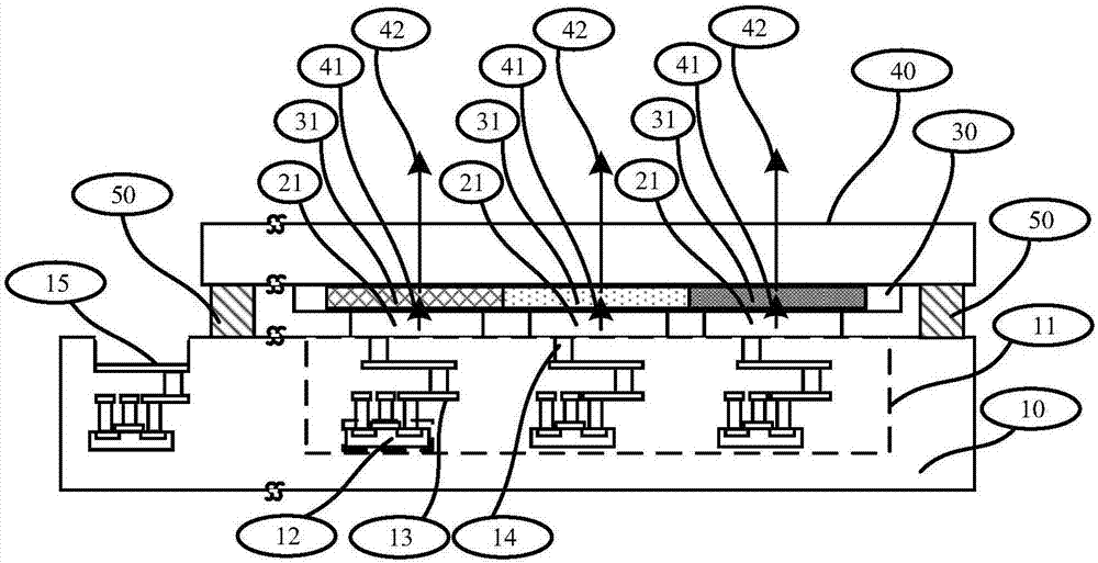
[0063] see figure 1 The full-color semiconductor light-emitting microdisplay is characterized in that it at least includes a silicon substrate 10, micro light-emitting diodes 21 arranged in an array, and a transparent substrate 40 with a color filter layer 30, and:

[0064] The silicon substrate includes a driving circuit 11, and the driving circuit 11 includes at least a metal-oxide semiconductor field effect transistor 12, a metal connection line 13, and a through hole 14. More specifically, the driving circuit 11 also includes an interface 15, which is used for external Bring in signals and power;

[0065] The micro light emitting diode 21 at least includes a first electrode 22, a multilayer non-organic compound 23 and a second electrode 24 (see Figure 8(a)-8(b) ), the non-organic compound 23 is composed of Ga, As, In, Al, Se, Zn, Si, P, N or C elements and can be doped; further, the non-organic compound is preferably GaAs, GaAsP, AlGaAs, AlGaInP , GaInN, AlGaP, AlGaN, G...

Embodiment 2

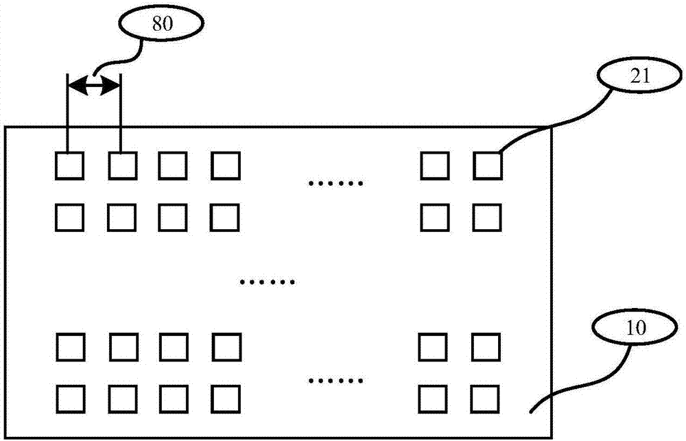
[0071] see figure 2 , this embodiment is basically the same as the first embodiment. Further, the center distance 80 between the micro-light emitting diodes 21 is not greater than 20 μm, preferably 5-10 μm in this embodiment, and the current of a single micro-light-emitting diode 21 is not higher than 30 μA. Embodiment preferred 1~5 μ A, thereby specified the pixel size size and the pixel current range of the full-color semiconductor light-emitting microdisplay of the present invention, and this is obviously smaller than the conventional display with glass as the substrate, making this embodiment very suitable for microdisplays .

Embodiment 3

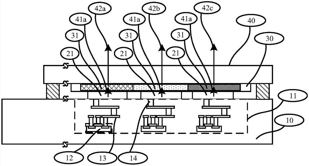
[0073] This embodiment is basically the same as the first embodiment. Further, the color filter point 31 completely covers the micro-LED 21 in the vertical direction, and the distance between the center point of the color filter point 31 and the center point of the micro-LED 21 is not greater than 1 μm, In this embodiment, it is preferably 0.5 μm, so that the pixel pitch can be reduced and the pixel aperture ratio can be increased within an optional process deviation range.


PUM


Abstract

The invention discloses a structure of a full-color semiconductor light emitting micro display and a manufacturing process thereof. The full-color semiconductor light emitting micro display comprises a silicon substrate, micro light emitting diodes arranged in an array and a transparent substrate with a color filter layer; each micro light emitting diode at least comprises a first electrode, a plurality of layers of non-organic compounds and a second electrode; the color filter layer is produced on the surface of the transparent substrate; the transparent substrate is adhered to the silicon substrate; the micro light emitting diodes are driven by a current provided by a driving circuit and emit first light; the color filter layer comprises a plurality of color filter points; and the color filter points cover the micro light emitting diodes in a vertical direction and convert the first light emitted by the micro light emitting diodes into second light. The manufacturing process of the full-color semiconductor light emitting micro display comprises the process of producing the driving circuit on the silicon substrate, producing the micro light emitting diodes on the silicon substrate on which the driving circuit is produced and adhering the transparent substrate on which the color filter layer is produced to the silicon substrate.

Description

technical field [0001] The invention relates to the technical field of manufacturing semiconductor light emitting microdisplays, in particular to a structure based on a micro light emitting diode device and a manufacturing process thereof. Background technique [0002] Light-emitting diode (LED) display technology based on non-organic light-emitting materials has been widely used in various industries. Most of the existing LEDs are based on sapphire, with a single pixel pitch of more than 100 microns, and are mainly used for medium and large-sized screens. In the field of wearable near-eye display and projection display, displays with smaller physical area, higher integration and higher resolution are expected, especially full-color micro-LED displays. LED microdisplays based on monocrystalline silicon are the best choice. However, the pixel pitch of most micro-LED displays is more than 30 microns at present, and most of them are monochrome devices, which cannot meet the r...

Claims


Application Information

Patent Timeline
Patent Type & Authority Applications(China)
IPC IPC(8): H01L27/15H01L21/77
CPCH01L27/1214H01L27/156H01L25/167H01L33/58
Inventor 黄舒平季渊穆廷洲
Owner 南京昀光科技有限公司
Why Eureka
Try Eureka