
Multiple-way switching PUF (physical unclonable function) circuit and serial number output circuit

A switching circuit and multi-channel switching technology, used in the protection of internal/peripheral computer components, etc., can solve the problems of unsatisfactory chip reliability uniqueness, increase system security, and low commercial possibility, and achieve uniqueness and reliability. The ideal value of the performance index, avoiding large errors, and reducing the risk of tape-out

Active Publication Date: 2017-09-29
View PDF5 Cites 0 Cited by
  • Summary
  • Abstract
  • Description
  • Claims
  • Application Information

AI Technical Summary

Problems solved by technology

In the existing PUF technology, PUF introduces a natural random source, which produces an almost unpredictable and replicable algorithm, increases system security, and also makes the serial number stored in the chip unable to be modified, erased and read at will
However, many chips manufactured using PUF technology have poor reliability, and tape-outs are prone to failure.
For example, the arbiter PUF generates multi-bit output values ​​by combining a single PUF circuit in parallel, but each delay path cannot communicate with each other, or the interconnection is less, if one of the delay paths has a large error that is different from other delay paths, it may be It will cause the output of the chip to be a fixed value that does not change according to the input, resulting in unsatisfactory reliability (Reliability) and uniqueness (Uniqueness) indicators of the chip, resulting in low commercial possibility and high risk

Method used


Image

  • Multiple-way switching PUF (physical unclonable function) circuit and serial number output circuit
  • Multiple-way switching PUF (physical unclonable function) circuit and serial number output circuit
  • Multiple-way switching PUF (physical unclonable function) circuit and serial number output circuit

Examples


Embodiment 1

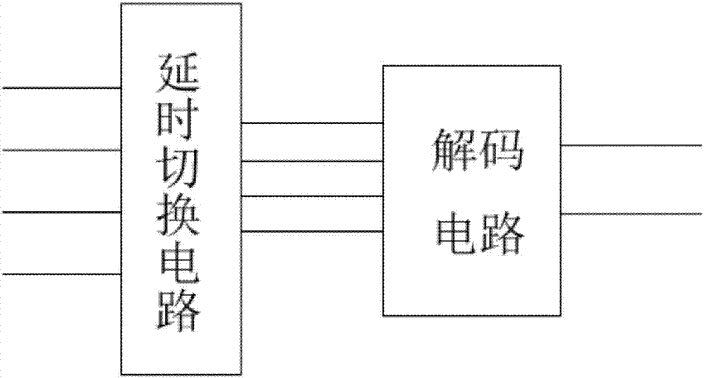
[0057] This embodiment describes in detail the structure and principle of a multiplexable PUF circuit provided by the present invention, see figure 1 , is a schematic diagram of the connection of the PUF circuit. The input and output terminals in the figure are only used to illustrate the connection relationship between the delay switching circuit and the decoding circuit. The specific number of input terminals and output terminals is not subject to the figure. PUF The circuit mainly includes:

[0058] Delay switching circuit, the delay switching circuit has a key input terminal, multiple signal input terminals and multiple signal output terminals, the key input terminal corresponds to the input of a two-digit key, and multiple signal input terminals are connected to the same external pulse signal , the delay switching circuit selects the same pulse signal input from different signal input terminals, converts the pulse signal into delayed signals of different rates, and output...

Embodiment 2

[0064] This embodiment is based on the content recorded in Embodiment 1, and describes in detail the PUF circuit that uses four data selectors to realize 4 delay paths. The larger errors generated during the process are dispersed inside the circuit, thereby improving randomness, reliability, and uniqueness.

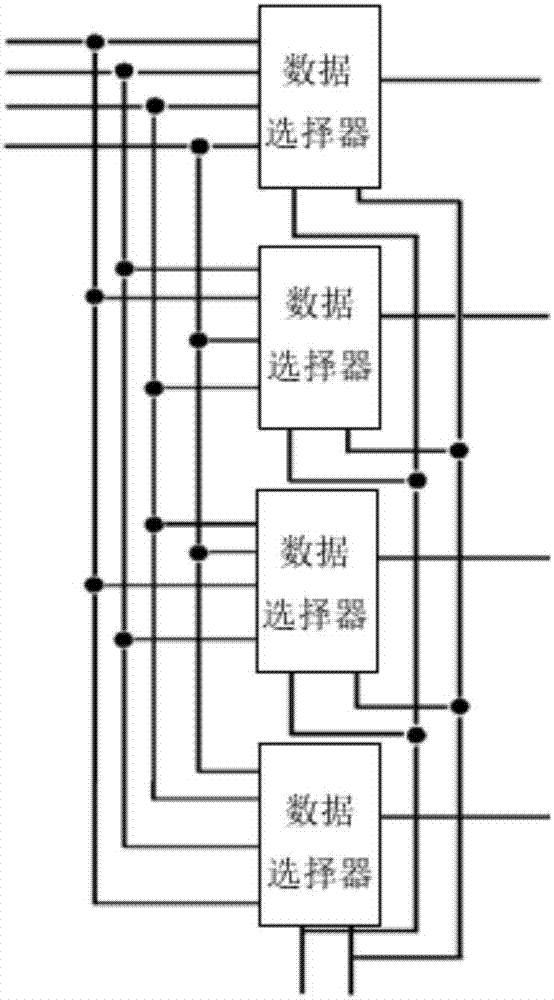
[0065] The connection relationship between the delay switching circuit and the decoding circuit has been stated in detail in Embodiment 1. On the basis of Embodiment 1, the delay switching circuit in the present embodiment selects four 4 to 1 data selectors to form, see Figure 4 , in addition, the principles of data selectors such as 2-to-1, 8-to-1, and 16-to-1 are similar, and details are not described here. For the convenience of explanation, the four data selectors are respectively named as the first data selector, the second data selector, the third data selector and the fourth data selector from top to bottom. The data input terminals of each data selector Accordin...

Embodiment 3

[0077] In order to further increase the randomness of the PUF circuit in the present invention, on the basis of Embodiment 1 and Embodiment 2, the signal input terminals and signal output terminals of n delay switching circuits can be connected in series sequentially, such as Figure 8 As shown, each delay switching circuit corresponds to the 2-bit input of the key, and n series delay switching circuits support the input of 2n-bit keys. It should be noted that the input key needs to follow the delay switching circuit. The connection sequence is from left to right, and from the lowest bit to the highest bit of the key, one unit per two bits is input to the key input terminal of the corresponding delay switching circuit.

[0078] The specific structures of the delay switching circuit and the decoding circuit in this embodiment have been specifically stated in Embodiment 1 and Embodiment 2, and will not be repeated here. Compared with embodiment 1 and embodiment 2, embodiment 3 i...


PUM


Abstract

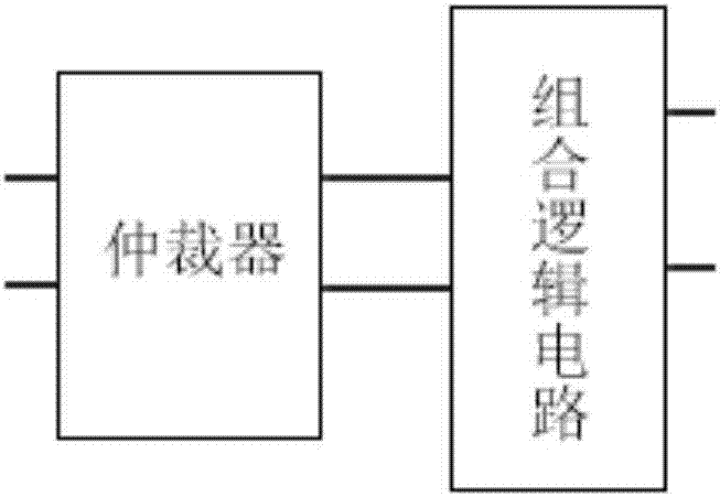
The invention relates to the technical field of integrated circuits, particularly to a multiple-way switching PUF circuit and a serial number output circuit. The multiple-way switching PUF circuit comprises a time-delay switching circuit and a decoding circuit, wherein the time-delay switching circuit selects the identical pulse signals input from different signal input ends, converts the pulse signals into delay signals of different rates and sequentially outputs the delay signals through different signal output ends; the input end of the decoding circuit is correspondingly connected with a plurality of signal output ends of the time-delay switching circuit, and according to the sequence that the delay signals output by the signal output ends reach the decoding circuit, processes the delay signal first reaching the decoding circuit to generate dual-bit output values, so that chips manufactured from the multiple-way switching PUF circuit obtain ideal indexes on randomness, uniqueness, reliability on the like and reduce tape-out risks. Besides, the invention also discloses a serial number output circuit composed of a plurality of connected PUF circuits, and accordingly the serial number output circuit obtains a serial number concealing and protecting function.

Description

technical field [0001] The invention relates to the technical field of integrated circuits, in particular to a multiplexable PUF circuit and a serial number output circuit. Background technique [0002] In the field of integrated circuits, the wafers and chips produced need to be marked with special unique serial numbers to distinguish the wafers or chips. In this technical field, the method for distinguishing the serial numbers of wafers and chips is in the Write a special serial number in EEPROM or EFLASH to achieve the purpose of distinction, but the serial number stored in the chip by this method is very easy to be modified or erased, and it is also easy to be read, which makes the chip easy to be deciphered. crack. [0003] In response to this situation, PUF technology came into being. PUF technology uses the unique physical characteristics of silicon wafers and the variability of IC manufacturing process to identify each chip, thereby judging the authenticity of the c...

Claims


Application Information

Patent Timeline
IPC IPC(8): G06F21/73
CPCG06F21/73
Inventor 徐咏丹周玉洁朱念好
Learn More