Post-processing method and application of double perovskite crystals

A double perovskite and crystal technology, which is applied in the field of post-processing of double perovskite crystals, can solve the problems of large leakage current, low carrier mobility and carrier lifetime product, limited preparation method, etc. The effect of improving performance, increasing mobility and defect density, reducing defect density

Active Publication Date: 2017-10-13
HUAZHONG UNIV OF SCI & TECH
View PDF3 Cites 20 Cited by
  • Summary
  • Abstract
  • Description
  • Claims
  • Application Information

AI Technical Summary

Problems solved by technology

Crystals with low leakage current and high μτ product are very beneficial for radiation detection, but limited by the preparation method, the current Cs 2 wxya 6 The crystal still has defects such as large leakage current and low product of carrier mobility and carrier lifetime (μτ) of the crystal, so it is very necessary to post-process the crystal to improve the radiation detection performance of the crystal
Currently, there is no Cs 2 wxya 6 Crystal post-processing method, therefore, it is very necessary to invent a post-processing method to improve the Cs 2 wxya 6 crystal quality

Method used


Image

  • Post-processing method and application of double perovskite crystals
  • Post-processing method and application of double perovskite crystals
  • Post-processing method and application of double perovskite crystals

Examples


Embodiment 1

[0029] Cs in this example 2 AgBr 6 The post-processing method of the crystal specifically includes the following steps:

[0030] (1) Use tweezers to remove the Cs grown in the solution 2 AgBr 6 take out;

[0031] (2) Cs to be taken out 2 AgBr 6 Place in an oven at 100°C, and anneal in air for 30 minutes;

[0032] (3) Take out the crystal in step (2) from the oven, and place it in the air to cool for 5 minutes;

[0033] (4) prepare a sufficient amount of isopropanol solution that can completely immerse the crystal;

[0034] (5) Soak the crystal in step (3) in the isopropanol solution prepared in step (4) for 10 min;

[0035] (6) Place the crystal in step (5) in the air to dry naturally, that is, complete the post-processing of the crystal, and take out the crystal for performance testing;

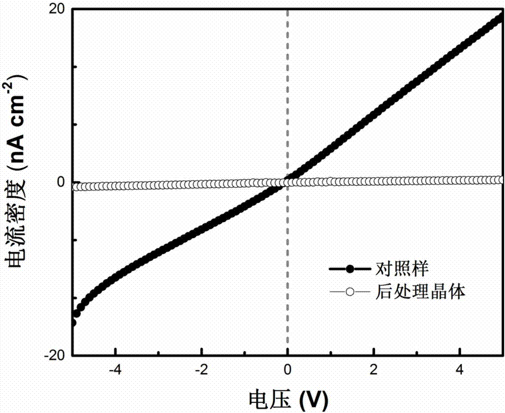
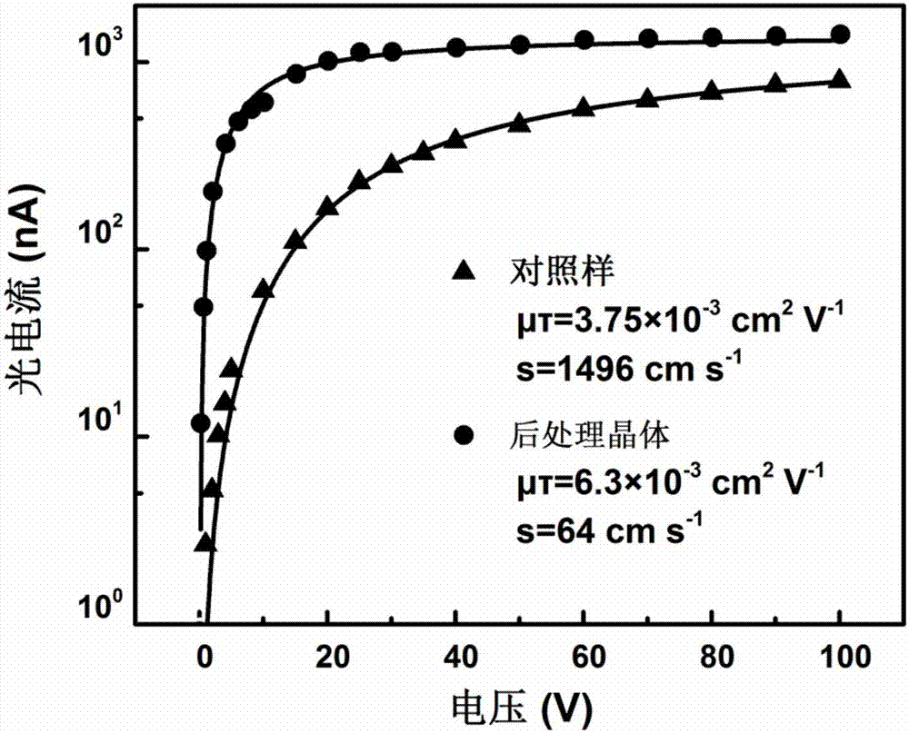
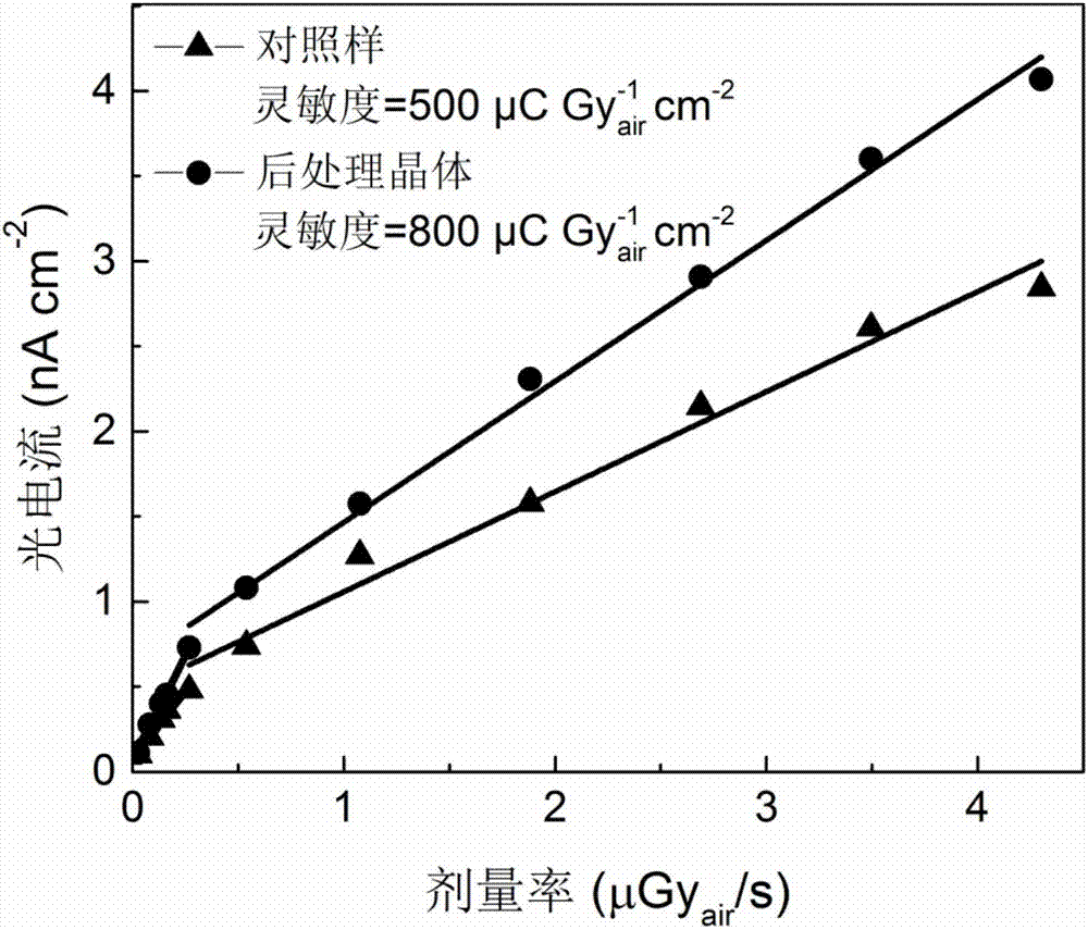
[0036] (7) Get post-treated crystals and no post-treated crystals, i.e. the control sample, vapor-deposit 40nm thick gold electrodes on its upper and lower surfaces, and perform a per...

Embodiment 2

[0041] (1) Use tweezers to remove the Cs grown in the solution 2 AgBr 6 take out;

[0042] (2) Cs to be taken out 2 AgBr 6 Placed in an oven at 200°C, and annealed in air for 120 minutes;

[0043] (3) The crystal in step (2) is taken out from the oven, and placed in the air to cool for 15 minutes;

[0044] (4) prepare a sufficient amount of ethanol solution that can completely immerse the crystal;

[0045] (5) Soak the crystal in step (3) in the ethanol solution prepared in step (4) for 15 minutes;

[0046] (6) Place the crystal in step (5) in the air to dry naturally, that is, complete the post-processing of the crystal, and take out the crystal for performance testing;

[0047] (7) Get post-treated crystals and no post-treated crystals, i.e. the control sample, vapor-deposit 40nm thick gold electrodes on its upper and lower surfaces, and perform a performance test;

[0048] (8) Use a semiconductor analyzer to carry out I-V tests on the above-mentioned post-treatment c...

Embodiment 3

[0052] (1) Use tweezers to remove the Cs grown in the solution 2 AgBiCl 6 take out;

[0053] (2) Cs to be taken out 2 AgBiCl 6 Place in an oven at 150°C, and anneal in air for 90 minutes;

[0054] (3) Take out the crystal in step (2) from the oven, and place it in the air to cool for 10 minutes;

[0055] (4) prepare a sufficient amount of acetone solution that can completely immerse the crystal;

[0056] (5) Soak the crystal in step (3) in the acetone solution prepared in step (4) for 10 min;

[0057] (6) Place the crystal in step (5) in the air to dry naturally, that is, complete the post-processing of the crystal, and take out the crystal for performance testing;

[0058] (7) Get post-treated crystals and no post-treated crystals, i.e. the control sample, vapor-deposit 40nm thick gold electrodes on its upper and lower surfaces, and perform a performance test;

[0059] (8) Use a semiconductor analyzer to carry out I-V tests on the above-mentioned post-treatment crystal...


PUM


Abstract

The invention discloses a post-processing method and application of double perovskite crystals. The post-processing method of double perovskite crystals comprises the following steps: performing annealing treatment on Cs2AgBiX6 double perovskite crystals; then cooling; and performing surface passivation treatment on the cooled crystals by means of a solvent to improve the mobility of the double perovskite crystals and reduce the surface recombination rate. The invention improves the technological process adopted in the key post-processing and the specific condition parameters adopted in each process step, therefore, the problems of the double perovskite Cs2AgBiX6 crystals in the prior art that the probability of occurrence of Ag and Bi dislocation is high, the internal defects of the crystals are more, the product of the carrier mobility multiply by the carrier lifetime ([mu] [tau]) of the crystals is not high are effectively solved; moreover, the crystals obtained by means of the post-processing method disclosed by the invention are especially suitable for using in radiation detectors.

Description

technical field [0001] The invention belongs to the field of post-treatment of double perovskite crystals, more specifically, relates to a post-treatment method and application of double perovskite crystals, the method can reduce double perovskite crystals (such as Cs 2 wxya 6 Crystal) defects, reduce the leakage current of the crystal, increase the μτ product (mobility × average life) of the crystal and reduce the surface recombination rate s. Background technique [0002] Cs 2 wxya 6 It is a perovskite material with superior photoelectric performance and large average atomic number, which is very suitable as a radiation detector material. Crystals with low leakage current and high μτ product are very beneficial for radiation detection, but limited by the preparation method, the current Cs 2 wxya 6 The crystal still has defects such as large leakage current and low product of carrier mobility and carrier lifetime (μτ) of the crystal, so it is very necessary to post-pro...

Claims


Application Information

Patent Timeline
Patent Type & Authority Applications(China)
IPC IPC(8): H01L31/18H01L31/09
CPCH01L31/09H01L31/18Y02P70/50
Inventor 唐江巫皓迪牛广达潘伟程罗家俊尹力骁
Owner HUAZHONG UNIV OF SCI & TECH
Why Eureka
Try Eureka