Method for manufacturing hole connecting layer, method for manufacturing circuit board and circuit board

A manufacturing method and connection layer technology, which are applied in the directions of electrical connection of printed components, formation of electrical connection of printed components, printed circuits, etc., can solve the problems of difficult control of copper thickness and uniformity of the outer layer of the daughter board, and prevent excessive glue flow. , the effect of improving the bonding strength

Active Publication Date: 2017-10-17
GUANGZHOU FASTPRINT CIRCUIT TECH +2
View PDF5 Cites 5 Cited by
  • Summary
  • Abstract
  • Description
  • Claims
  • Application Information

AI Technical Summary

Problems solved by technology

[0004] However, the traditional Via bond process still has defects: when the sub-board is made of POFV (plated on filled via, electroplating on the hole) process, it is difficult to control the thickness and uniformity of the outer layer of the sub-board copper, which is generally controlled at an average value of 30 μm to 40 μm. Range ±5μm

Method used


Image

  • Method for manufacturing hole connecting layer, method for manufacturing circuit board and circuit board
  • Method for manufacturing hole connecting layer, method for manufacturing circuit board and circuit board
  • Method for manufacturing hole connecting layer, method for manufacturing circuit board and circuit board

Examples


Embodiment Construction

[0033] In order to make the objectives, technical solutions, and advantages of the present invention clearer, the following further describes the present invention in detail with reference to the accompanying drawings and specific embodiments. It should be understood that the specific embodiments described herein are only used to explain the present invention, and do not limit the protection scope of the present invention.

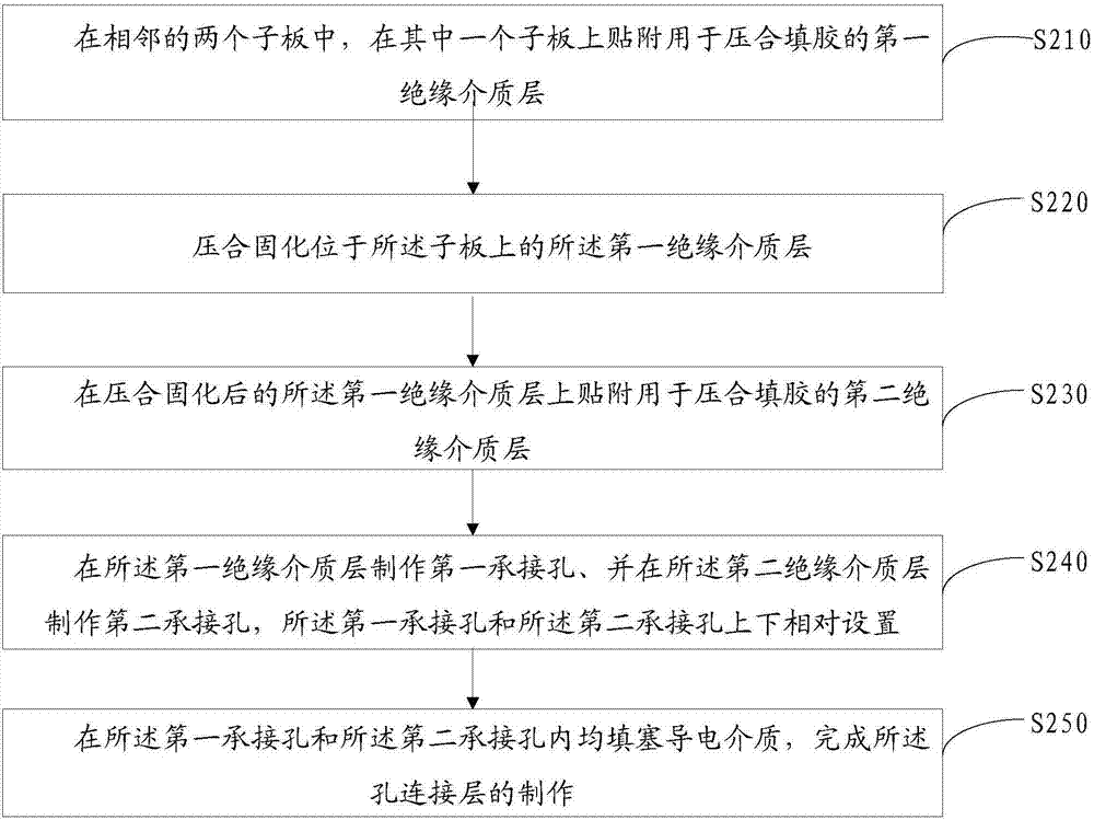
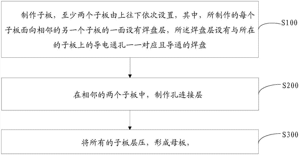
[0034] The mother board is generally formed by laminating at least two daughter boards 100 stacked one above the other, and a via bond layer (via bond layer) is provided between two adjacent daughter boards 100. Such as figure 1 with Image 6 As shown, the manufacturing method of the hole connecting layer of the present invention includes the following steps:

[0035] In S210, in two adjacent sub-boards 100, a first insulating dielectric layer 200 for pressing and filling is attached to the side of one sub-board 100 facing the other adjacent sub-board 100.

[00...


PUM


Abstract

The invention discloses a method for manufacturing a hole connecting layer, a method for manufacturing a circuit board and a circuit board. The method for manufacturing a hole connecting layer comprises: attaching one daughter board to a first insulating dielectric layer for pressing a filter; pressing and solidifying the first insulating dielectric layer arranged on the daughter board; pasting a second insulating dielectric layer for pressing a filler on the first insulating dielectric layer after pressing and solidifying; manufacturing a first carrying hole in the first insulating dielectric layer and manufacturing a second carrying hole opposite to the first carrying hole in an up-down manner in the second insulating dielectric layer; and filling the first carrying hole and the second carrying hole with conductive media to complete manufacturing of a hole connecting layer. Therefore, the dual-sided filler filing need can be met; the bonding strength of the adjacent daughter boards is enhanced; the fluidity of the hole connecting hole is controlled; a phenomenon that the carrying hole shape is damaged by too large flowing glue can be avoided; and the conducting media can be protected from being squeezed and dispersed.

Description

Technical field [0001] The invention relates to the technical field of printed circuit boards, in particular to a method for manufacturing a hole connecting layer, a method for manufacturing a circuit board, and a circuit board. Background technique [0002] With the development and construction of the communications industry, high-level digital backplanes have been gradually applied. With the increase of various networked consumer products in the future, greater capacity and higher speed will be required for information transmission. The construction of future 5G networks will inevitably require backplanes that can carry more daughter boards, with less signal loss, and higher reliability. The realization of ultra-high-density, higher-layer backplane manufacturing technology will be a development direction of the printed circuit industry in the future. [0003] Via bond (hole connection) technology is an arbitrary interconnection technology between Z-direction layers. It is to r...

Claims


Application Information

Patent Timeline
Patent Type & Authority Applications(China)
IPC IPC(8): H05K3/42H05K1/11
CPCH05K1/115H05K3/429H05K2201/095H05K3/4614H05K2203/061H05K3/0047H05K3/027H05K3/4611
Inventor 廉泽阳吴森李艳国陈蓓
Owner GUANGZHOU FASTPRINT CIRCUIT TECH
Why Eureka
Try Eureka