Semiconductor structure and manufacturing method thereof

A manufacturing method and semiconductor technology, applied in the fields of semiconductor/solid-state device manufacturing, semiconductor devices, electrical components, etc., can solve problems such as poor electrical performance of semiconductor devices, and achieve the effect of improving electrical performance and avoiding influences

Inactive Publication Date: 2017-10-24
SEMICON MFG INT (SHANGHAI) CORP +1
View PDF3 Cites 4 Cited by
  • Summary
  • Abstract
  • Description
  • Claims
  • Application Information

AI Technical Summary

Problems solved by technology

[0006] However, the electrical performance of the semiconductor device formed by the prior art is poor

Method used


Image

  • Semiconductor structure and manufacturing method thereof
  • Semiconductor structure and manufacturing method thereof
  • Semiconductor structure and manufacturing method thereof

Examples


Embodiment Construction

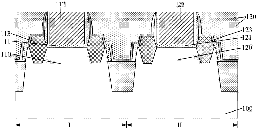
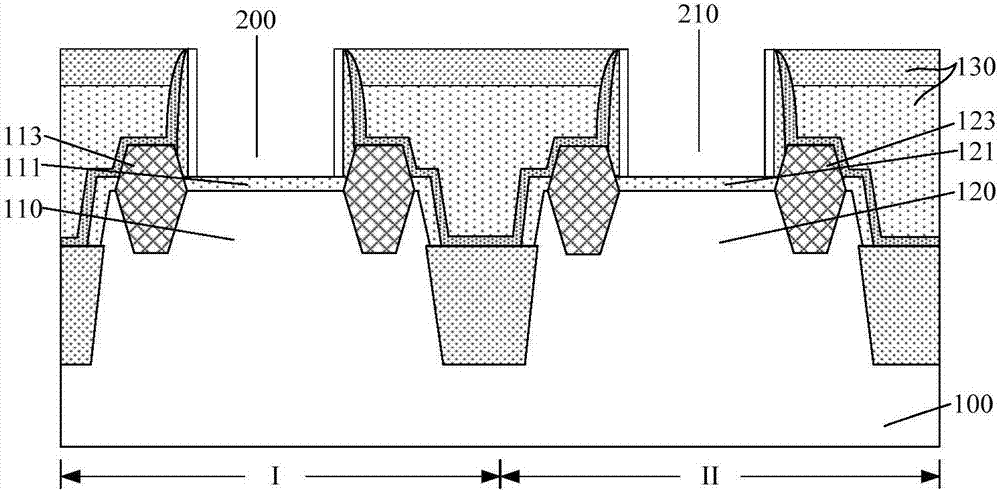
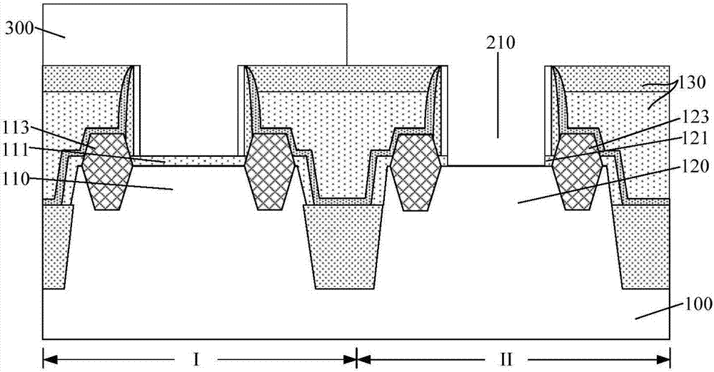
[0014] The electrical performance of the semiconductor device in the prior art is poor, and the reason is analyzed in combination with the manufacturing method of the semiconductor structure. refer to Figure 1 to Figure 5 , shows a structural schematic diagram corresponding to each step of a manufacturing method of a semiconductor structure in the prior art. The manufacturing method of described semiconductor structure comprises the following steps:

[0015] refer to figure 1 , forming a semiconductor base, the semiconductor base includes a substrate 100, fins protruding from the substrate 100; the substrate 100 includes a first region I and a second region II, protruding from the first region I The fin of the substrate 100 is the first fin 110 , and the fin protruding from the second region II of the substrate 100 is the second fin 120 . The first region I is used to form peripheral devices, and the second region II is used to form core devices.

[0016] Specifically, th...


PUM


Abstract

The invention discloses a semiconductor structure and a manufacturing method thereof. The manufacturing method comprises the steps of forming a substrate including a first region and a second region and fin portions protruding out of the substrate; forming a first pseudo gate structure at the surface of the fin portion in the first region, wherein the first pseudo gate structure comprises a gate oxide layer and a first pseudo gate electrode layer; forming a second pseudo gate structure at the surface of the fin portion in the second region, wherein the second pseudo gate structure comprises a gate oxide layer and a second pseudo gate electrode layer; forming a dielectric layer; removing the first pseudo gate electrode layer, and forming a first opening in the dielectric layer; forming a compensation side wall at the side wall of the first opening; removing the second pseudo gate structure, and forming a second opening in the dielectric layer; forming a gate dielectric layer at the surface of the gate oxide layer, the side wall of the compensation side wall and the bottom and the side wall of the second opening; and filling a metal layer in the first opening and the second opening. The compensation side wall covers a damaged part of the gate oxide layer, so that the damaged part of the gate oxide layer is enabled to become a non-effective gate oxide layer above a channel region, and thus the electrical property of the device is improved.

Description

technical field [0001] The invention relates to the field of semiconductors, in particular to a semiconductor structure and a manufacturing method thereof. Background technique [0002] In semiconductor manufacturing, with the development trend of VLSI, the feature size of integrated circuits continues to decrease. In order to adapt to the reduction of feature size, the channel length of MOSFET field effect transistors is also continuously shortened accordingly. However, as the channel length of the device is shortened, the distance between the source and the drain of the device is also shortened, so the control ability of the gate to the channel becomes worse, and the gate voltage pinches off the channel. The difficulty is also increasing, making the phenomenon of subthreshold leakage (subthreshold leakage), the so-called short-channel effect (SCE: short-channel effects) more likely to occur. [0003] Therefore, in order to better adapt to the reduction of feature size, t...

Claims


Application Information

Patent Timeline
Patent Type & Authority Applications(China)
IPC IPC(8): H01L21/336H01L29/78H01L21/28H01L29/423
CPCH01L21/28H01L21/28008H01L29/4232H01L29/42364H01L29/66795H01L29/785
Inventor 周飞
Owner SEMICON MFG INT (SHANGHAI) CORP
Why Eureka
Try Eureka