Insulating ring, pre-cleaning chamber and semiconductor processing equipment

A technology for processing equipment and insulating rings, which is applied in the manufacture of semiconductor/solid-state devices, discharge tubes, electrical components, etc., can solve the problems of increasing the etching rate at the edge of the wafer, increasing the bombardment energy, and affecting the etching uniformity. Achieve the effect of improving etching uniformity, reducing etching rate and reducing variance

Inactive Publication Date: 2017-10-24
BEIJING NAURA MICROELECTRONICS EQUIP CO LTD
View PDF7 Cites 2 Cited by
  • Summary
  • Abstract
  • Description
  • Claims
  • Application Information

AI Technical Summary

Problems solved by technology

As can be seen from the figure, the etching rate of the wafer edge region (A region) is obviously higher than that of the central region, and this is because the electric field strength distributed at the edge of the wafer 9 and the contact position of the base 7 is to

Method used


Image

  • Insulating ring, pre-cleaning chamber and semiconductor processing equipment
  • Insulating ring, pre-cleaning chamber and semiconductor processing equipment
  • Insulating ring, pre-cleaning chamber and semiconductor processing equipment

Examples


Embodiment Construction

[0026] In order for those skilled in the art to better understand the technical solution of the present invention, the insulating ring, the pre-cleaning chamber and the semiconductor processing equipment provided by the present invention will be described in detail below with reference to the accompanying drawings.

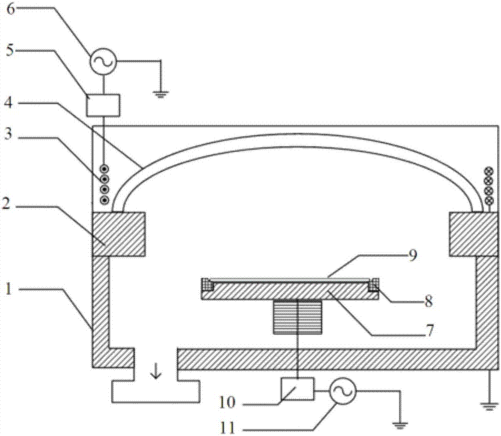
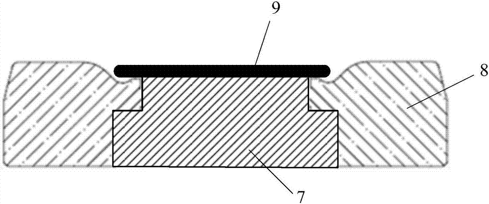
[0027] Figure 4 A cross-sectional view of an insulating ring provided by an embodiment of the present invention. see Figure 4 , the insulating ring 12 is applied in a pre-cleaning chamber (not shown in the figure), and the pre-cleaning chamber is used to remove impurities on the surface of the wafer by an etching process, and it includes a base 10, which includes a base for carrying The first bearing surface 101 in the central area of ​​the lower surface of the wafer 11 , and the annular groove, which is arranged at the edge of the first bearing surface 101 .

[0028] The insulating ring 12 includes an annular body, which is arranged on the above-mentioned ann...


PUM


Abstract

The invention provides an insulating ring, a pre-cleaning chamber and semiconductor processing equipment. The insulating ring is applied to the pre-cleaning chamber. A base is arranged in the pre-cleaning chamber; the base comprises a first bearing surface for bearing the center area of the lower surface of a wafer; the insulating ring is arranged on the base and surrounds the edge of the first bearing surface; the insulating ring comprises a ring-shaped body, the ring-shaped body is provided with a second bearing surface and a ring-shaped boss, the second bearing surface and the edge area of the lower surface of the wafer are arranged oppositely, the ring-shaped boss surrounds the edge of the second bearing surface, and the upper surface of the ring-shaped boss is higher than that of the wafer. According to the insulating ring provided in the invention, the etching rate of the edge area of the wafer can be reduced, the difference between the etching rate of the edge area of the wafer and the etching rate of the center area of the wafer can be reduced, and the etching uniformity can be further improved.

Description

technical field [0001] The invention relates to the technical field of semiconductor manufacturing, in particular to an insulating ring, a pre-cleaning chamber and semiconductor processing equipment. Background technique [0002] The pre-cleaning technology has been widely used in semiconductor manufacturing processes, especially for integrated circuits, through-silicon vias and other manufacturing processes. The purpose of pre-cleaning is to remove the contamination and impurities on the surface of the wafer, so as to facilitate the effective progress of the subsequent deposition process and ensure the overall performance of the integrated circuit device. [0003] Commonly used pre-cleaning chambers usually adopt inductively coupled plasma (ICP) processing equipment. The basic principle is to use high-voltage alternating electric fields generated by radio frequency power sources to excite process gases (such as argon, helium, hydrogen and oxygen, etc.) to form Plasma, ions...

Claims


Application Information

Patent Timeline
IPC IPC(8): H01L21/67H01J37/32
CPCH01L21/67028H01J37/321H01J37/32431H01L21/67069H01L21/6719
Inventor 徐奎常大磊陈鹏
Owner BEIJING NAURA MICROELECTRONICS EQUIP CO LTD
Why Eureka
Try Eureka