Display device, array substrate, thin film transistor, and manufacturing method thereof

A technology of thin film transistors and insulating layers, which is applied in the direction of transistors, semiconductor/solid-state device manufacturing, electric solid-state devices, etc., and can solve the problem of low deposition rate

Inactive Publication Date: 2017-10-24
SHENZHEN CHINA STAR OPTOELECTRONICS SEMICON DISPLAY TECH CO LTD
View PDF2 Cites 0 Cited by
  • Summary
  • Abstract
  • Description
  • Claims
  • Application Information

AI Technical Summary

Problems solved by technology

[0004] The technical problem mainly solved by the present invention is to provide a display device, an array substrate, a thin-film transistor and a manufacturing method thereof, which solve the problem of low deposition rate while improving the reliability of the transistor, and improve production efficiency

Method used


Image

  • Display device, array substrate, thin film transistor, and manufacturing method thereof
  • Display device, array substrate, thin film transistor, and manufacturing method thereof
  • Display device, array substrate, thin film transistor, and manufacturing method thereof

Examples


Embodiment Construction

[0015] The present invention will be described in detail below with reference to the accompanying drawings and embodiments.

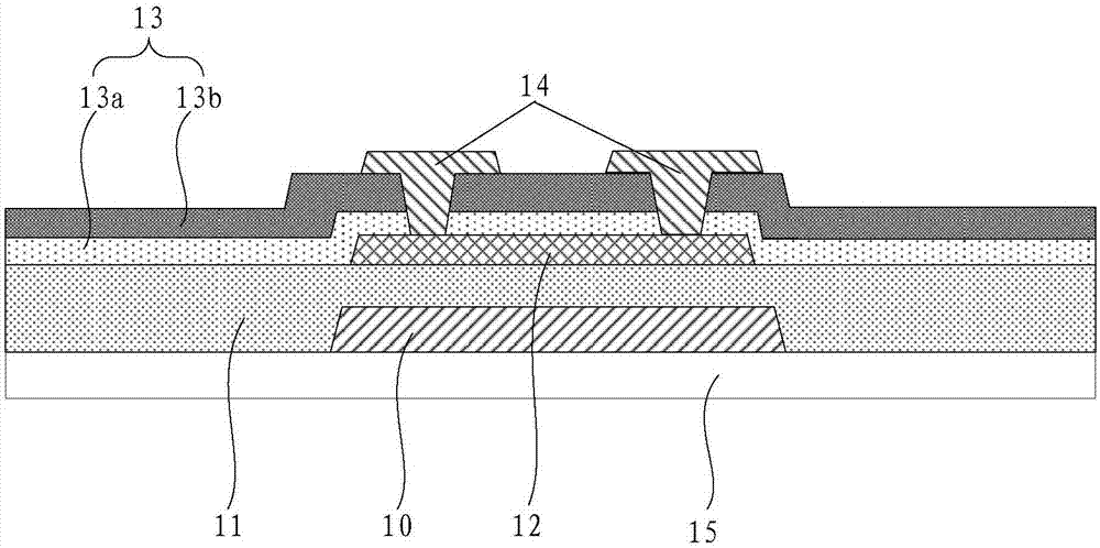
[0016] see figure 1 , figure 1 It is a schematic structural diagram of an embodiment of the thin film transistor of the present invention. The thin film transistor includes: a gate electrode layer 10 , a first insulating layer 11 , an active layer 12 , a passivation layer 13 , and source and drain electrode layers 14 . A first insulating layer 11 covers the gate electrode layer 10, an active layer 12 is formed on the first insulating layer 11, a passivation layer 13 covers the active layer 12, and source and drain electrode layers 14 are formed on the passivation layer 13 . The passivation layer 13 includes a second insulating layer 13a and a third insulating layer 13b, wherein the second insulating layer 13a is disposed close to the active layer 12 and is processed by an atomic layer deposition process, and the third insulating layer 13b covers the s...


PUM


Abstract

The invention discloses a display device, an array substrate, a thin film transistor, and a manufacturing method thereof. The thin film transistor comprises a gate electrode layer, a first insulating layer, an active layer, a passivation layer, a source electrode, and a drain electrode layer. The passivation layer comprises a second insulating layer and a third insulating layer. The second insulating layer is close to the active layer and the passivation layer is treated by an atom layer sedimentation technique. A third insulating layer is covered on the second insulating layer is treated by a plasma-enhanced chemical vapor deposition process. Through the above method, the thin film transistor solves a problem of low deposition rate while improving reliability of the transistor, and improves production efficiency.

Description

technical field [0001] The present invention relates to the technical field of flat panel display, in particular to a display device, an array substrate, a thin film transistor and a manufacturing method thereof. Background technique [0002] Flat-panel display devices have many advantages such as thin body, power saving, and no radiation, and have been widely used. Existing flat panel display devices mainly include liquid crystal display devices (Liquid Crystal Display, LCD) and organic light emitting diode display devices (Organic Light Emitting Display, OLED), and active matrix organic light emitting diodes (Active-matrix organic light emitting diode, AMOLED) has significant advantages over LCD in terms of energy consumption, color saturation, contrast, flexible applications, etc., and is widely used. [0003] During long-term research and development, the inventors of the present application found that the oxide thin film transistor (Oxide TFT) technology has a problem ...

Claims


Application Information

Patent Timeline
Patent Type & Authority Applications(China)
IPC IPC(8): H01L29/786H01L21/34H01L27/12
CPCH01L29/7869H01L27/1214H01L29/66969
Inventor 刘兆松
Owner SHENZHEN CHINA STAR OPTOELECTRONICS SEMICON DISPLAY TECH CO LTD
Why Eureka
Try Eureka