Copper-clad ceramic substrate manufacturing method

A technology of copper-clad ceramic substrate and manufacturing method, which is applied in printed circuit manufacturing, electrical components, printed circuits, etc., can solve the problems of increasing environmental pressure, inconvenient recycling, complex process, etc., to reduce the pressure of wastewater treatment and facilitate recycling. , the effect of good isolation performance

Inactive Publication Date: 2017-10-24
SHUNSIN TECH (ZHONG SHAN) LTD
View PDF4 Cites 7 Cited by
  • Summary
  • Abstract
  • Description
  • Claims
  • Application Information

AI Technical Summary

Problems solved by technology

Due to the complexity of the etching process and the need for more materials and equipment input, the manufacturing process of copper-clad ceramic substrates in the prior art has the following defects: 1. The process is complicated, and many types of materials and equipment are required, and the economy is not good; 2. A large amount of copper is dissolved i

Method used


Image

  • Copper-clad ceramic substrate manufacturing method
  • Copper-clad ceramic substrate manufacturing method
  • Copper-clad ceramic substrate manufacturing method

Examples


Embodiment Construction

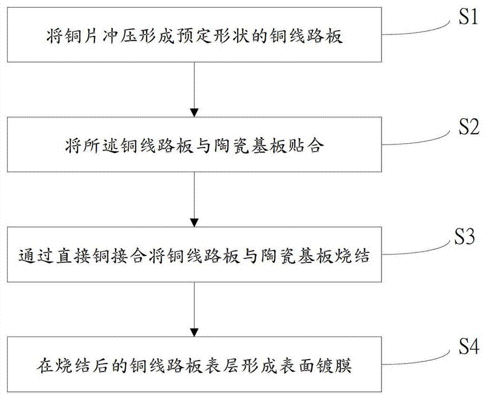
[0020] refer to image 3 As shown, the manufacturing method of the copper-clad ceramic substrate disclosed in the present invention comprises:

[0021] S1, stamping the copper sheet to form a copper circuit board 1 of a predetermined shape;

[0022] S2, laminating the copper circuit board 1 and the ceramic substrate 2;

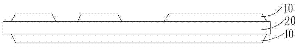
[0023] S3 , sintering the copper circuit board 1 and the ceramic substrate 2 by direct bonding copper (Direct Bonding Copper, DBC). The copper circuit board 1 formed by stamping has neat side walls and is perpendicular to the ceramic 2 substrate, has good isolation performance, and has a simple process and low cost. In specific implementation, the copper circuit board 1 and the ceramic substrate 2 can be sintered by heating oxidation method, wherein the oxidation temperature is 950°C-1100°C, and the oxidation time is 20min-35min. During the heating oxidation process, the oxidation atmosphere can be preferably It is a weak oxygen atmosphere under the protect...


PUM

PropertyMeasurementUnit
Thicknessaaaaaaaaaa

Abstract

The invention discloses a copper-clad ceramic substrate manufacturing method. The method comprises steps: a copper sheet is stamped to form a copper circuit board in a predetermined shape; the copper circuit board and the ceramic substrate are attached; and through direct copper joint, the copper circuit board and the ceramic substrate are sintered. According to the copper-clad ceramic substrate manufacturing method disclosed in the invention, the processing process is simplified, steps such as film mounting, exposure, development, etching and film removal in the existing processing process are cancelled, needed materials and device kinds are reduced, and the economical efficiency is improved; stamping to form the copper circuit board is used to replace the etching process, copper material recovery and utilization are facilitated, the pressure of wastewater treatment is reduced, and the method is environment-friendly; and besides, the copper circuit board formed through stamping is good in circuit perpendicularity, and the isolation performance is good.

Description

technical field [0001] The invention relates to the technical field of ceramic substrate metallization, in particular to a method for manufacturing a copper-clad ceramic substrate. Background technique [0002] Direct copper bonding technology, referred to as DBC (Direct Bonding Copper), is heat treatment in a temperature range lower than the melting point of metallic copper (about 1083°C) and higher than the eutectic temperature of copper and copper oxide (about 1063°C) , a technical means to make the external structure and copper produce eutectic bonding and fixed connection. Copper clad ceramic substrate is a typical product using direct copper bonding technology, which is mainly used in the field of product packaging with high power and high heat dissipation requirements. [0003] figure 1 It is a typical processing flow chart of the copper-clad ceramic substrate in the prior art, figure 2 for with figure 1 Schematic diagram of the structure of the corresponding cop...

Claims


Application Information

Patent Timeline
IPC IPC(8): H05K3/20
CPCH05K3/20H05K2203/033H05K1/0306H05K2203/1131H05K3/381H05K3/385H05K2203/0315
Inventor 任飞
Owner SHUNSIN TECH (ZHONG SHAN) LTD
Why Eureka
Try Eureka