Array substrate, manufacturing method thereof and display panel
A technology for array substrates and display panels, which is applied in the manufacture of semiconductor/solid-state devices, electrical components, and electrical solid-state devices, etc., can solve the problems of high cathode resistance, affecting the display quality of light-emitting devices, and voltage drop.
- Summary
- Abstract
- Description
- Claims
- Application Information
AI Technical Summary
Problems solved by technology
Method used
Image

Examples
Embodiment 1
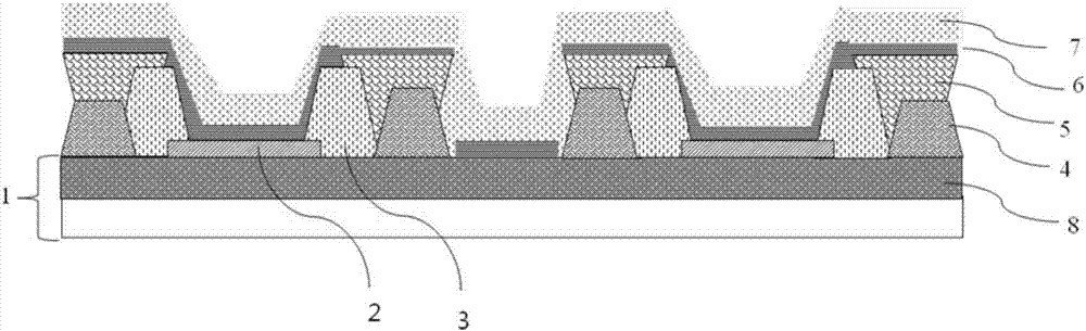
[0038] see figure 1 , which shows a structural block diagram of an array substrate according to Embodiment 1 of the present invention, specifically including:
[0039] A substrate 1 , an anode layer 2 , a first pixel defining layer 3 , an auxiliary cathode layer 4 , a second pixel defining layer 5 , an organic light emitting layer 6 and a cathode layer 7 .
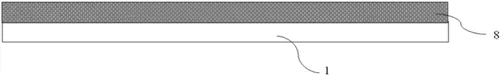
[0040] In practical applications, the substrate 1 may be a BP substrate with a thin film transistor array fabricated, and may also include a planarization layer 8 formed on the BP substrate. The material of the planarization layer may be resin, polyimide, organic silicon, silicon dioxide and other materials, or silicon nitride material, which is not specifically limited in the present invention.
[0041] Then the anode layer 2 , the first pixel defining layer 3 and the auxiliary cathode layer 4 are sequentially patterned on the substrate 1 .
[0042] Wherein, the first pixel defining layer 3 divides a plurality of pixel ...
Embodiment 2
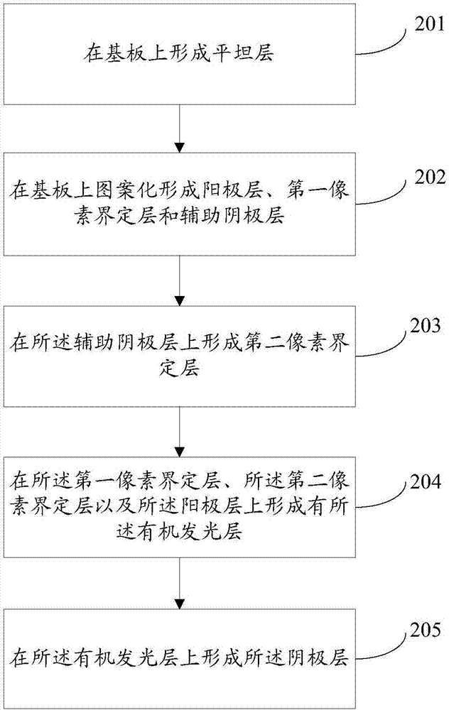
[0054] refer to figure 2 , which shows a flowchart of a method for preparing an array substrate according to Embodiment 2 of the present invention, specifically including:
[0055] Step 201: providing a substrate.
[0056] A flat layer 8 may be pre-formed on the substrate 1, such as image 3 shown.
[0057] The material of the planarization layer may be resin, polyimide, organic silicon, silicon dioxide and other materials, or silicon nitride material, which is not specifically limited in the present invention.
[0058] Before forming the planar layer, the following steps may also be included: forming a gate layer, a gate insulating layer, an active layer, an etching stopper layer, a passivation layer, and a resin layer on the substrate.
[0059] Specifically, a TFT pattern with a thickness of 1um-100um is formed by repeating film formation, exposure, etching, and development processes on the substrate many times. Common film formation processes include sputtering (Sputter...
Embodiment 3
[0079] The present invention also discloses a display panel, including the array substrate in the first embodiment.
[0080] It should be noted that the display panel in this embodiment can be any product or component with a display function such as a mobile phone, a tablet computer, a television, a notebook computer, a digital photo frame, and a navigator.
[0081] The display panel has all the advantages of the array panel in the first embodiment above, and will not be repeated here.
PUM
| Property | Measurement | Unit |
|---|---|---|
| Thickness | aaaaa | aaaaa |
| Thickness | aaaaa | aaaaa |
| Thickness | aaaaa | aaaaa |
Abstract
Description
Claims
Application Information
 - Generate Ideas
- Intellectual Property
- Life Sciences
- Materials
- Tech Scout
- Unparalleled Data Quality
- Higher Quality Content
- 60% Fewer Hallucinations
Browse by: Latest US Patents, China's latest patents, Technical Efficacy Thesaurus, Application Domain, Technology Topic, Popular Technical Reports.
© 2025 PatSnap. All rights reserved.Legal|Privacy policy|Modern Slavery Act Transparency Statement|Sitemap|About US| Contact US: help@patsnap.com