Top-emitting organic electroluminescence diode display device and manufacture method therefor

A luminescence and top-emission technology, which is applied in the direction of organic semiconductor devices, semiconductor/solid-state device manufacturing, electric solid-state devices, etc., can solve the problems of open circuit metal, uneven brightness of display screen, and inability to form ohmic contact, etc., to reduce resistance, The effect of increasing the image refresh rate

Inactive Publication Date: 2017-11-10
BOE TECH GRP CO LTD
View PDF10 Cites 13 Cited by
  • Summary
  • Abstract
  • Description
  • Claims
  • Application Information

AI Technical Summary

Problems solved by technology

Commonly used cathode materials such as Al, Mg-Ag, and Ag can have good light transmittance only when they are very thin, but too thin a cathode layer will lead to open circuit or metal oxidation, and cannot form an effective ohmic contact, resulting in the brightness of the display screen. Uneven

Method used


Image

  • Top-emitting organic electroluminescence diode display device and manufacture method therefor
  • Top-emitting organic electroluminescence diode display device and manufacture method therefor
  • Top-emitting organic electroluminescence diode display device and manufacture method therefor

Examples


Embodiment 1

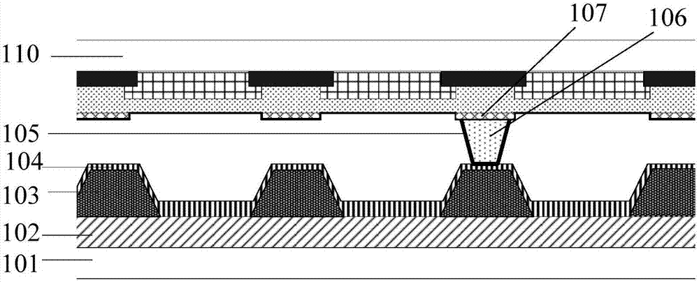
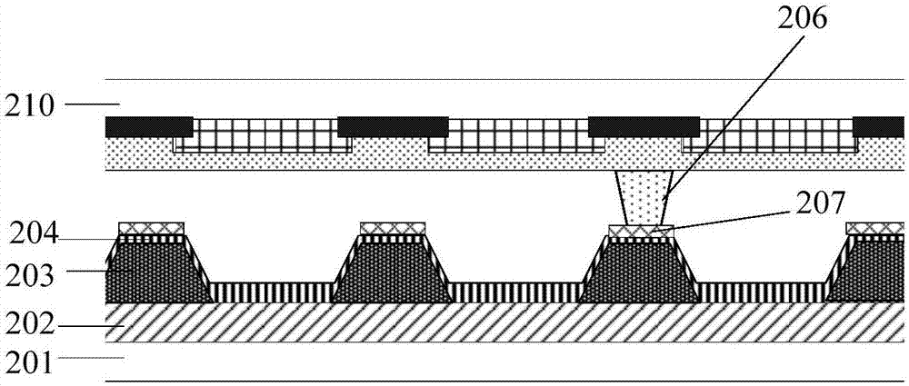
[0027] This embodiment provides a top emission organic electroluminescent diode display device. image 3 is a schematic structural view showing a top emission organic electroluminescent diode display device according to an embodiment of the present invention.

[0028] Such as image 3 As shown, the top emission organic electroluminescent diode display device includes: a glass substrate 201, a thin film transistor substrate 202 arranged on the glass substrate; a pixel definition layer 203, arranged on the thin film transistor substrate 202, an organic light emitting layer (not shown in the figure) out), arranged on the thin film transistor substrate; the cathode layer 204 is arranged on the organic light-emitting layer, covering the pixel definition layer 203, and the cathode auxiliary layer 207 is arranged on the cathode layer 204, and the position of the cathode auxiliary layer 207 is the same as that of the The positions of the pixel definition layer 203 correspond to each ...

Embodiment 2

[0034] This embodiment provides a method for manufacturing a top emission organic electroluminescent diode display device. Figure 4 It is a process flow diagram showing a method for manufacturing a top emission organic electroluminescent diode display device according to an embodiment of the present invention.

[0035] Such as Figure 4 As shown, the method includes the following steps.

[0036] In step S401 , forming a thin film transistor substrate includes cleaning the substrate by a standard method, and performing a preparation process of the thin film transistor.

[0037] In step S402, a pixel definition layer and an organic light emitting layer are formed on the thin film transistor substrate. It includes: coating a layer of light-curing material in a spin coating manner, with a thickness between 1.6 microns and 2.0 microns. Pre-baking, exposure, development, post-baking, and patterning processes are performed to prepare a pixel definition layer; and an organic light...


PUM


Abstract

The invention provides a top-emitting organic electroluminescence diode display device and a manufacture method therefor. The device comprises a film transistor substrate; an organic light-emitting layer which is disposed on the film transistor substrate; a cathode layer which is disposed on the organic light-emitting layer; a cathode auxiliary layer which is disposed on the cathode layer; a cover plate which is opposite to the film transistor substrate; and an underlay object which is disposed on one surface, opposite to the film transistor substrate, of the cover plate, and makes contact with the cathode auxiliary layer. According to the invention, the device employs the 3D printing technology, can reduce the resistance of the cathode layer on the film transistor substrate through the combination of the cathode auxiliary layer with larger thickness with the cathode layer, improves the image refreshing frequency, and cannot affect the light transmittance.

Description

technical field [0001] The invention relates to the field of display technology, in particular to a top-emitting organic electroluminescent diode display device and a manufacturing method thereof. Background technique [0002] At present, organic electroluminescent display (OLED) is emerging in the field of flat panel display with the characteristics of thinness, low power consumption, high response, and high resolution, and its potential market prospect is optimistic by the industry. Top-emitting AMOLED (active organic electroluminescent diode) can effectively solve the problems of reduced aperture ratio and display brightness reduction caused by complex TFT (thin film field-effect transistor) compensation circuits. The existing microcavity effect can also improve the color gamut of the AMOLED display and improve the display effect. [0003] As the top-emitting AMOLED must project part, the light transmittance and conductivity of the transparent cathode are crucial factors...

Claims


Application Information

Patent Timeline
Patent Type & Authority Applications(China)
IPC IPC(8): H01L51/52H01L27/32H01L51/56
CPCH10K59/1315H10K50/824H10K71/00H10K2102/3026
Inventor 李伟谢蒂旎张星
Owner BOE TECH GRP CO LTD
Why Eureka
Try Eureka