Method for manufacturing flexible backplane, liquid crystal display panel and OLED display panel
A manufacturing method and backplane technology, applied in the direction of climate sustainability, final product manufacturing, sustainable manufacturing/processing, etc., can solve the problems of reducing product yield, damaging the active layer, etc., and achieve the effect of improving flexibility
- Summary
- Abstract
- Description
- Claims
- Application Information
AI Technical Summary
Problems solved by technology
Method used
Image

Examples
Embodiment Construction
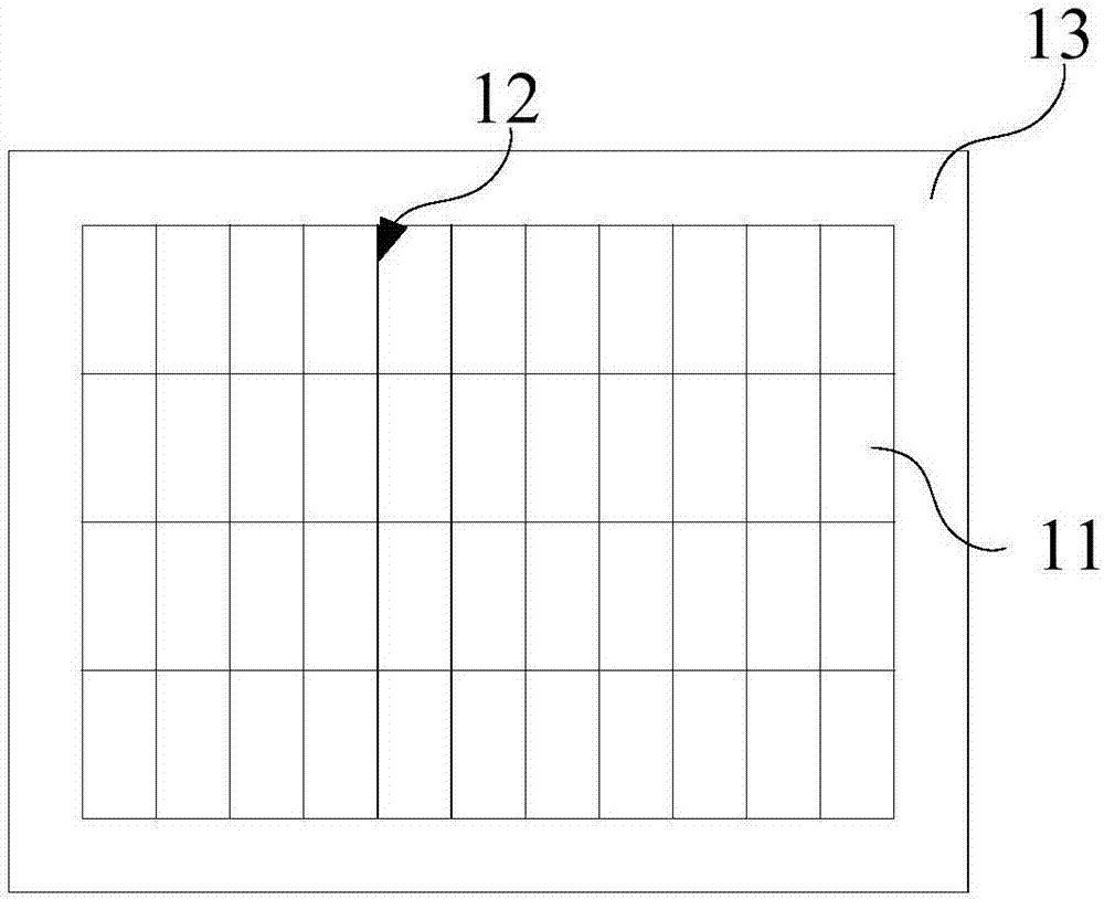
[0020] refer to figure 1 , figure 1 It is a structural schematic diagram of an embodiment of a manufacturing method of a flexible backplane provided by the present invention. The flexible backplane includes a plurality of pixel regions 11 , an isolation region 12 between the plurality of pixel regions 11 and a binding region 13 .
[0021] Among them, a plurality of pixel regions 11 are distributed in an array to form an AA (Active Area) region of the backplane, and an isolation region 12 is formed between two adjacent pixel regions 11. It is worth noting that the isolation region 12 is only used for Isolating the TFTs of two pixels does not separate the two pixels.
[0022] Wherein, the binding area (ie, bongding area) 13 is generally located at the edge of the display panel, and is used for setting various circuits, such as driving circuits.
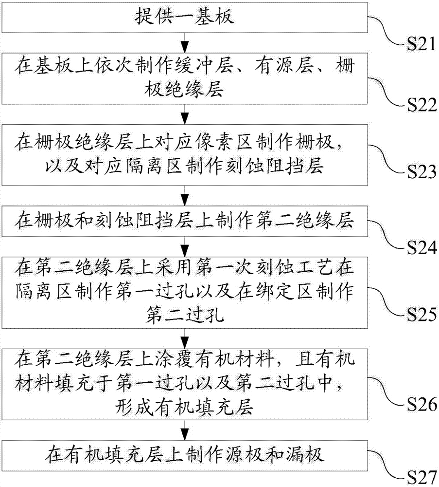
[0023] It can be understood that in the manufacturing process of the following embodiments, each interlayer structure of the backpla...
PUM
 Abstract
Description
Claims
Application Information
 - Generate Ideas
- Intellectual Property
- Life Sciences
- Materials
- Tech Scout
- Unparalleled Data Quality
- Higher Quality Content
- 60% Fewer Hallucinations
Browse by: Latest US Patents, China's latest patents, Technical Efficacy Thesaurus, Application Domain, Technology Topic, Popular Technical Reports.
© 2025 PatSnap. All rights reserved.Legal|Privacy policy|Modern Slavery Act Transparency Statement|Sitemap|About US| Contact US: help@patsnap.com