Test structure, test probe card, test system and test method

A test structure and test probe technology, which is applied in the field of semiconductors, can solve the problems of WAT test accuracy to be improved, and achieve the effects of reduced test cost, improved test accuracy, and improved test accuracy

Active Publication Date: 2020-03-10
SEMICON MFG INT (SHANGHAI) CORP +1
View PDF8 Cites 0 Cited by
  • Summary
  • Abstract
  • Description
  • Claims
  • Application Information

AI Technical Summary

Problems solved by technology

[0003] However, with the continuous reduction of device feature size, the accuracy of WAT testing needs to be improved

Method used


Image

  • Test structure, test probe card, test system and test method
  • Test structure, test probe card, test system and test method
  • Test structure, test probe card, test system and test method

Examples


Embodiment Construction

[0019] The test accuracy of the prior art is low, combined with reference figure 1 and figure 2 , shows a schematic diagram of an embodiment of the prior art testing method. Analyze the reasons for this:

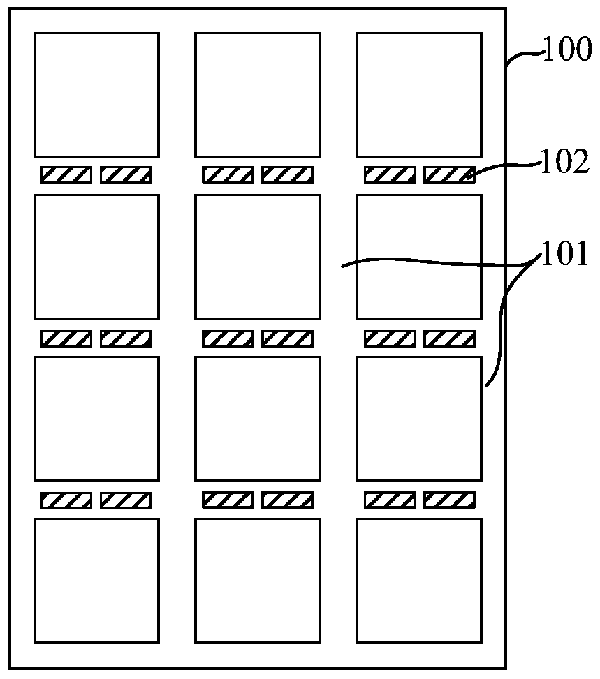
[0020] Such as figure 1 As shown, several test structures 102 are located within the dicing line 101 of the wafer 100 . In the prior art, a probe card (not shown) is usually used for testing, and after the test of a test structure 102 is completed, the probe card is moved from the test structure 102 to the next structure to be tested 102 positions And continue to test until all test structures 102 are tested.

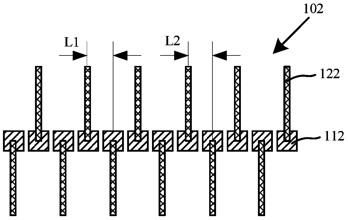
[0021] Specifically, as figure 2 As shown, the test structure 102 includes a plurality of test pads 112 , and the probe card includes a plurality of probes 122 . Wherein, the number of the test pads 112 is equal to the number of the probes 122 , and the probes 122 are in contact with the test pads 112 in a one-to-one correspondence. At present, the number of ...


PUM


Abstract

A test structure, a test probe card, a test system and a test method are provided. The test structure includes a plurality of bonding pads arranged in a line, including a first common bonding pad, a second common bonding pad adjacent to the first common bonding pad, a third common bonding pad located on a far side of the second common bonding pad away from the first common bonding pad, a fourth common bonding pad located on a far side of the third common bonding pad away from the second common bonding pad and adjacent to the third common bonding pad, and a plurality of test bonding pads located between the second common bonding pad and the third common bonding pad; and a plurality of test devices correspondingly connected with the test bonding pads, wherein, the test devices connected with the test bonding pads of an odd number are first devices and the test devices connected with the test bonding pads of an even number are second devices. The probe card includes a plurality of probes with the number being half the number of bonding pads. Compared with the prior art, the probe card enables the distance between the adjacent probes to be doubled and the number to be half the number of bonding pads, the leakage current during the test is reduced, and the manufacturing cost of the probe card is also reduced.

Description

technical field [0001] The invention relates to the field of semiconductors, in particular to a test structure, a test probe card, a test system and a test method. Background technique [0002] With the continuous advancement of technology in the semiconductor field, in order to know the yield rate of wafers in a timely manner during the production process, it is necessary to perform WAT (Wafer Acceptance Test, Wafer Acceptance Test) tests on wafers, and pass the detected data through the WAT Alg platform The output and storage are convenient for technicians to control the production of wafers to ensure the yield rate of wafers in production. [0003] However, with the continuous reduction of device feature size, the accuracy of WAT testing needs to be improved. Contents of the invention [0004] The problem to be solved by the present invention is to provide a test structure, a test probe card, a test system and a test method to improve test accuracy. [0005] To solve ...

Claims


Application Information

Patent Timeline
Patent Type & Authority Patents(China)
IPC IPC(8): G01R31/26G01R1/073
CPCG01R1/07342G01R31/2601
Inventor 竹敏
Owner SEMICON MFG INT (SHANGHAI) CORP
Why Eureka
Try Eureka