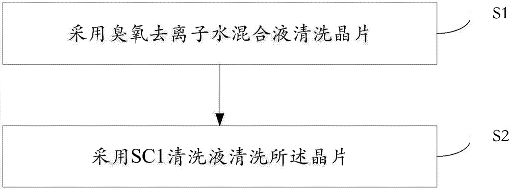
Method for cleaning chip
A technology for cleaning wafers and wafers, which is applied in the direction of electrical components, semiconductor/solid-state device manufacturing, circuits, etc., can solve the problems that cannot meet the requirements of the cleaning process, and achieve the effect of avoiding cross-infection and easy removal
- Summary
- Abstract
- Description
- Claims
- Application Information
AI Technical Summary
Problems solved by technology
Method used
Image

Examples
Embodiment 1
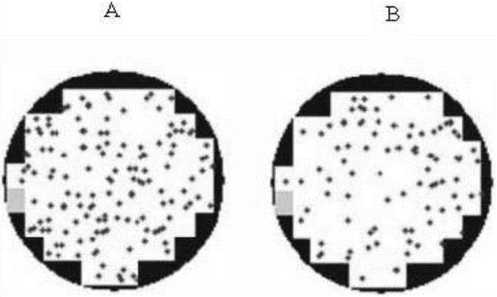
[0029] Before growing a thin film on a wafer, a cleaning process is usually performed to ensure the cleanliness of the wafer and avoid buried particle defects caused by unclean cleaning after the thin film grows, which will affect the yield of the wafer. In this embodiment, it is applied to the wafer cleaning process before the film growth, and is especially suitable for the wafer cleaning before the film growth through the furnace tube equipment.
[0030] In the present embodiment, the cleaning method of the present invention is adopted to oxidize the wafer or the film structure formed on the wafer by using Ozone. Specifically, Ozone can be sprayed on the upper and lower surfaces of the wafer to make the oxide layer on the wafer thicker. , or oxidize some attached particles, and then, when cleaning the wafer with SC1 cleaning solution, the oxide layer is removed, and at the same time, the attachments on the wafer surface will be removed together. Before the wafer is cleaned, ...
Embodiment 2
[0042] Photoresist is the blocking sacrificial layer in the ion implantation or etching process. After the ion implantation or etching process is completed, a cleaning process is required. In the cleaning process, the photoresist should be cleaned. At the same time, the photoresist The lower film layer structure loss is less. In the prior art, the cleaning methods of SPM and SC1 are adopted. In this method, the structure under the photoresist will be lost.
[0043] In this embodiment, the wafer cleaning method of the present invention can be used to oxidize the organic photoresist by using Ozone, and the oxidized photoresist will be cleaned more easily during SC1 cleaning. Complete removal of the photoresist can be achieved, avoiding excessive loss of the film layer structure under the photoresist.
[0044] In this embodiment, the photoresist can be a mask layer in the ion implantation process, for example, it can be a mask layer when performing well doping, source-drain dopi...
Embodiment 3
[0047] Dry etching is a method of etching thin films by plasma. During the etching process, the plasma reacts with the thin film to generate volatile substances, so as to achieve the purpose of etching. At the same time of etching, organic matter will be generated By-products, therefore, after dry etching, a cleaning process is required. In the cleaning process, the by-products should be cleaned, and at the same time, the loss of the film itself should be less. In the prior art, the cleaning methods of SPM and SC1 are adopted, and in this method, the loss of the film itself will be caused.
[0048] In this embodiment, using the wafer cleaning method of the present invention, the by-products of organic matter can be oxidized by using Ozone, and the by-products after oxidation will be cleaned more easily during SC1 cleaning. Therefore, a shorter time is used. The complete removal of by-products can be achieved, and excessive loss of the film itself can be avoided.
[0049] The ...
PUM
 Abstract
Description
Claims
Application Information
 - Generate Ideas
- Intellectual Property
- Life Sciences
- Materials
- Tech Scout
- Unparalleled Data Quality
- Higher Quality Content
- 60% Fewer Hallucinations
Browse by: Latest US Patents, China's latest patents, Technical Efficacy Thesaurus, Application Domain, Technology Topic, Popular Technical Reports.
© 2025 PatSnap. All rights reserved.Legal|Privacy policy|Modern Slavery Act Transparency Statement|Sitemap|About US| Contact US: help@patsnap.com