

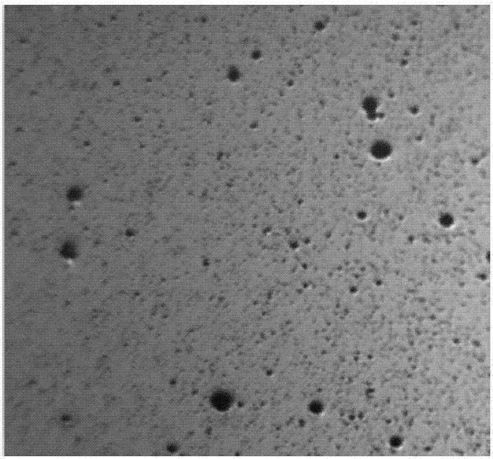
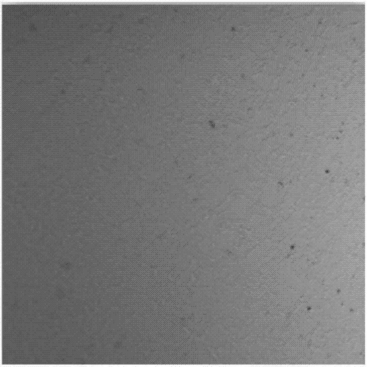
Method for improving surface microdefects of Si modified layer of large-diameter SiC mirror
A micro-defect, silicon carbide technology, used in coating, sputtering, metal material coating processes, etc., can solve problems affecting mirror roughness and smoothness, improve polishing characteristics, reduce surface micro-defects, and prepare The effect of process simplification
- Summary
- Abstract
- Description
- Claims
- Application Information
AI Technical Summary
Problems solved by technology
Method used
Image

Examples
Embodiment 1
[0038] The method for improving the microscopic defects on the surface of the silicon modified layer of the large-diameter silicon carbide mirror of the present invention comprises the following specific steps:
[0039] Step 1. Preparation of coating conditions: install the Si target on the sputtering cathode, fix the RB-SiC substrate after surface cleaning on the workpiece fixture of the coating machine, and evacuate the vacuum chamber of the coating machine to 4.5×10 -4 Pa, bake at a temperature of 200°C and keep the temperature constant for 90 minutes;
[0040] Step 2, sputtering cathode Si target surface treatment: pass high-purity Ar gas into the sputtering cathode, adjust the Ar gas flow to 400 sccm, adjust the sputtering cathode power to 3KW, and the sputtering time to 50 minutes to make the high-energy Ar + Ions bombard the target surface;
[0041] Step 3, prepare the Si modified layer: adjust the power of the sputtering cathode to 15KW, adjust the Ar gas flow to 550 ...
Embodiment 2
[0045] The method for improving the microscopic defects on the surface of the silicon modified layer of the large-diameter silicon carbide mirror of the present invention comprises the following specific steps:
[0046] Step 1. Preparation of coating conditions: install the Si target on the sputtering cathode, fix the RB-SiC substrate after surface cleaning on the workpiece fixture of the coating machine, and evacuate the vacuum chamber of the coating machine to 5.0×10 -4 Pa, bake at a temperature of 180°C and keep the temperature constant for 60 minutes;
[0047] Step 2, sputtering cathode Si target surface treatment: pass high-purity Ar gas into the sputtering cathode, adjust the Ar gas flow rate to 350 sccm, adjust the sputtering cathode power to 2KW, and the sputtering time to 40 minutes to make the high-energy Ar + Ions bombard the target surface;
[0048] Step 3, prepare the Si modified layer: adjust the power of the sputtering cathode to 12KW, adjust the Ar gas flow to...
Embodiment 3
[0051] The method for improving the microscopic defects on the surface of the silicon modified layer of the large-diameter silicon carbide mirror of the present invention comprises the following specific steps:
[0052] Step 1. Preparation of coating conditions: install the Si target on the sputtering cathode, fix the RB-SiC substrate after surface cleaning on the workpiece fixture of the coating machine, and evacuate the vacuum chamber of the coating machine to 4.0×10 -4 Pa, bake at a temperature of 220°C and keep the temperature constant for 120 minutes;
[0053] Step 2, sputtering cathode Si target surface treatment: pass high-purity Ar gas into the sputtering cathode, adjust the Ar gas flow rate to 550 sccm, adjust the sputtering cathode power to 4KW, and the sputtering time to 60 minutes to make the high-energy Ar + Ions bombard the target surface;
[0054] Step 3, prepare the Si modified layer: adjust the power of the sputtering cathode to 18KW, adjust the Ar gas flow t...
PUM
| Property | Measurement | Unit |
|---|---|---|
| thickness | aaaaa | aaaaa |
| surface roughness | aaaaa | aaaaa |
| surface roughness | aaaaa | aaaaa |
Abstract
Description
Claims
Application Information