Power semiconductor device with charge balance design

A semiconductor and body technology, applied in the field of drift region structure, can solve the problems of high on-state loss, poor diode reverse recovery softness, poor electrical performance compromise, etc.

Active Publication Date: 2017-12-01
INFINEON TECH AG
View PDF12 Cites 4 Cited by
  • Summary
  • Abstract
  • Description
  • Claims
  • Application Information

AI Technical Summary

Problems solved by technology

However, these approaches generally lead to poorer electrical performance tradeoffs, such as poorer diode reverse recovery...

Method used


Image

  • Power semiconductor device with charge balance design
  • Power semiconductor device with charge balance design
  • Power semiconductor device with charge balance design

Examples


Embodiment Construction

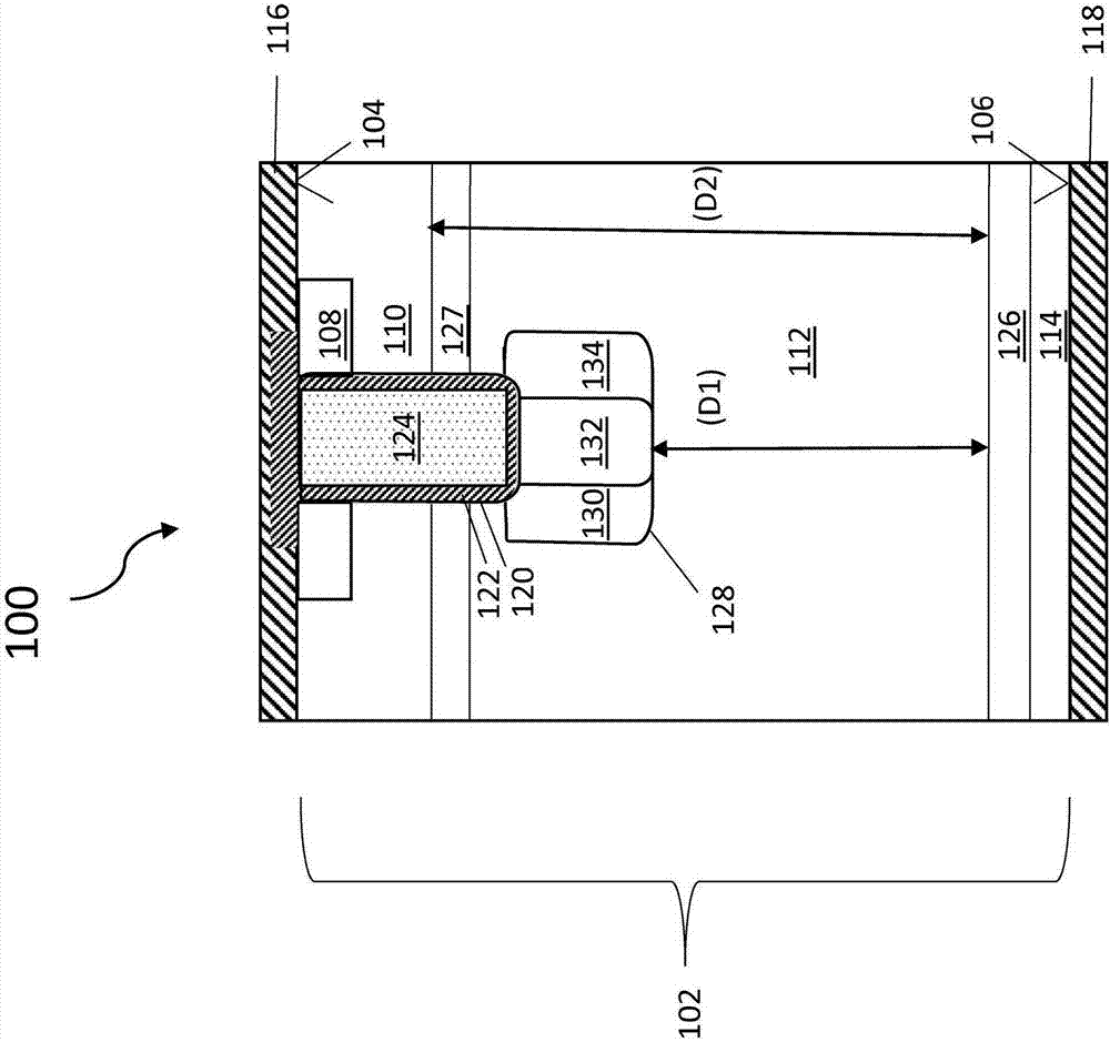
[0027]Embodiments disclosed herein include power semiconductor devices. According to one embodiment, the power semiconductor device is an IGBT with a vertical trench gate electrode structure. The power semiconductor device includes a doped superjunction region arranged at the bottom of the gate trench and extending vertically into the drift region of the device. The doped superjunction region comprises three doped pillars or stripes of alternating conductivity type (ie p-n-p or n-p-n). The doped superjunction region extends vertically no more than half of the drift region.

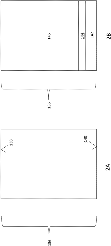
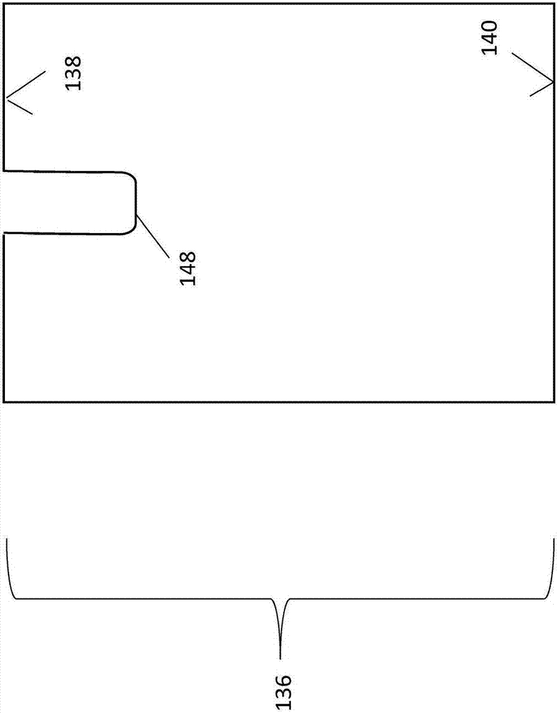
[0028] Various methods for forming power semiconductor devices are disclosed. Embodiments of these methods include providing a lightly doped first semiconductor layer of the first conductivity type. A doped superjunction region is formed in the first semiconductor layer. Various different techniques are disclosed for forming doped superjunction regions in the first semiconductor layer. One technique i...


PUM


Abstract

An embodiment of the invention relates to a power semiconductor device with a charge balance design. A semiconductor body having first and second vertically spaced apart surfaces is formed. A gate trench that vertically extends from the first surface of the semiconductor body towards the second surface is formed. A gate electrode and a gate dielectric are formed in the gate trench. The gate dielectric electrically insulates the gate electrode from adjacent semiconductor material. A doped superjunction region vertically extending from a bottom of the gate trench towards the second surface of the semiconductor body is formed. The doped superjunction region includes first, second, and third doped pillars vertically extending from the first surface of the first semiconductor layer and directly adjoining one another. The second pillar is laterally centered between the first and third pillars and has an opposite conductivity type as the first and third pillars.

Description

technical field [0001] The present application relates to power semiconductor devices, and more particularly to drift region structures that enhance the electrical performance of power semiconductor devices. Background technique [0002] Power semiconductor devices, particularly field-effect controlled switching devices such as metal-oxide-semiconductor field-effect transistors (MOSFETs) or insulated-gate bipolar transistors (IGBTs), have been used in a variety of applications, including but not limited to as power supplies and switches in power converters, electric vehicles, air conditioners and even stereo systems. Especially with regard to power devices capable of switching high currents and / or operating at higher voltages, low on-state resistance Ron, high breakdown voltage U bd and / or high robustness. A power MOSFET generally includes a drain region, a drift region adjacent to the drain region, and a source region, each region having a first conductivity type, and the...

Claims


Application Information

Patent Timeline
IPC IPC(8): H01L21/331H01L23/552H01L29/06H01L29/739
CPCH01L23/552H01L29/0634H01L29/0684H01L29/66348H01L29/7397H01L29/7398H01L29/7813H01L21/0465H01L29/1608H01L29/66068H01L29/66734H01L29/0878H01L29/0638H01L29/1095
Inventor 谢佩珊H-J·舒尔策
Owner INFINEON TECH AG
Why Eureka
Try Eureka