

Image collector and fingerprint collection device
An image collector and image sensor technology, which is applied in printing image collection, image communication, fingerprint/palmprint acquisition/organization, etc., can solve the problems of large image collector thickness and high production cost, and achieve simple production, low cost, The effect of simple production process
- Summary
- Abstract
- Description
- Claims
- Application Information
AI Technical Summary
Problems solved by technology
Method used
Image

Examples
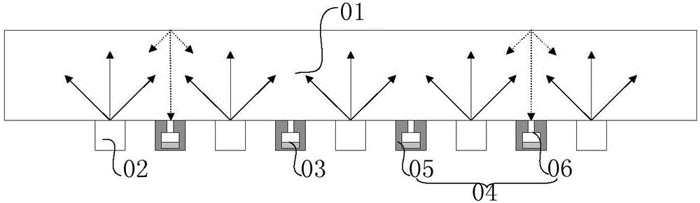
no. 1 example
[0022] figure 2 It is a schematic structural diagram of an image collector shown in the first embodiment. Such as figure 2 As shown, the image collector includes a transparent cover 11, an image sensor 12 arranged below the transparent cover 11, and a light blocking layer 13 arranged above the transparent cover 11; the image sensor 12 is provided with several photosensitive pixels 15 , the light-blocking layer 13 is provided with several small light-transmitting holes 14 .
[0023] The light blocking layer 13 is made of opaque material. Preferably, the light-blocking layer 13 is a light-blocking film; in actual processing, the light-blocking layer 13 can be coated on the transparent cover plate 11 by vapor deposition or electroplating, and the light-transmitting small holes on the light-blocking layer 13 14 is formed by etching process. In practical application, the thickness of the light blocking layer 13 is less than 100um.
[0024] In the present embodiment, the imag...
no. 2 example
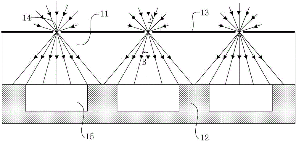
[0033] Figure 4 is a schematic structural diagram of the image collector shown in the second embodiment. Such as Figure 4As shown, the image collector provided in this embodiment includes an image sensor 21, a first transparent medium layer 23, a light blocking layer 22, a second transparent medium layer 24, a third transparent medium layer 25 and a fourth transparent medium layer from bottom to top. Layer 26, wherein the thickness of the first transparent medium layer 23 is h 1 .
[0034] The light-blocking layer 22 is made of opaque material, and several light-transmitting small holes 27 are arranged on its surface. In actual processing, the light-blocking layer 22 can be made by vapor deposition or electroplating, and the light-transmitting holes 27 on the light-blocking layer 22 can be made by etching.
[0035] According to the law of refraction of light, a ray of refraction index n A The medium A propagates to the refractive index n B Refraction occurs when the me...
no. 3 example
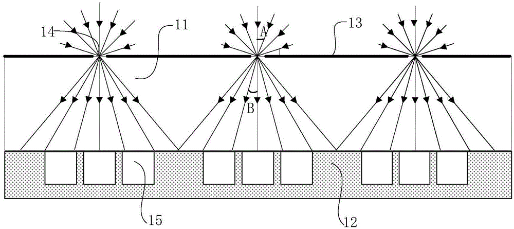
[0050] Figure 5 is a schematic structural diagram of the image collector shown in the third embodiment. Such as Figure 5 As shown, this embodiment and Figure 4 The structures and functions of the corresponding embodiments are basically the same, except that the second transparent medium layer 24 and the third transparent medium layer 25 are located below the light blocking layer 22 in this embodiment. Such as Figure 5 As shown, the image-side field of view formed by the small light-transmitting hole 27 on the image sensor 21 is also limited.
[0051] Of course, in other embodiments, the number and thickness of the transparent medium layers can be adjusted as required. For example, the first transparent medium layer 23 can be canceled; perhaps, the second transparent medium layer 24 can be canceled; or, the first transparent medium layer 23 and the second transparent medium layer 24 can be canceled at the same time; perhaps, the fourth transparent medium layer 26 can be...
PUM
| Property | Measurement | Unit |
|---|---|---|
| Thickness | aaaaa | aaaaa |
Abstract
Description
Claims
Application Information