Supercharge Your Innovation With Domain-Expert AI Agents!

Semiconductor device and packaging method thereof

A packaging method and semiconductor technology, applied in the field of micro-electromechanical systems, can solve the problems of complex packaging process and low integration, and achieve the effect of simple and convenient process

Active Publication Date: 2020-07-31
ZHEJIANG JUEXIN MICROELECTRONICS CO LTD
View PDF7 Cites 0 Cited by
  • Summary
  • Abstract
  • Description
  • Claims
  • Application Information

AI Technical Summary

Problems solved by technology

[0004] The purpose of the present invention is to provide a semiconductor device and its packaging method, which solves the problems of complex packaging process and low integration in the prior art

Method used


Image

  • Semiconductor device and packaging method thereof
  • Semiconductor device and packaging method thereof
  • Semiconductor device and packaging method thereof

Examples


Embodiment Construction

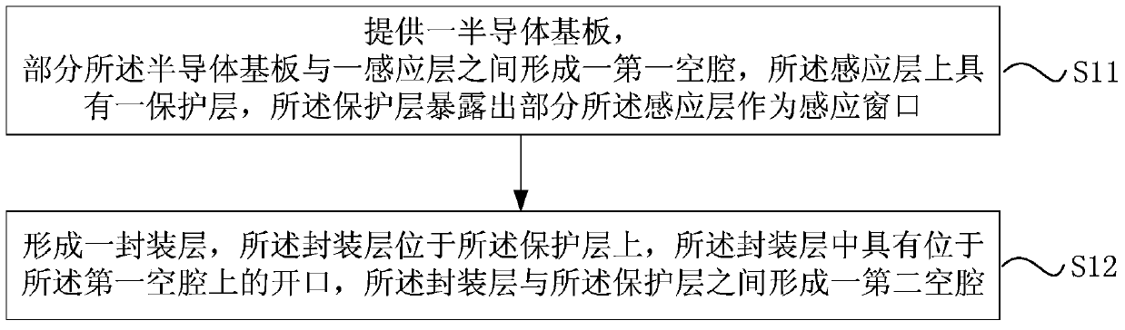
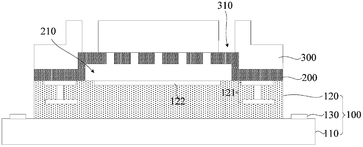
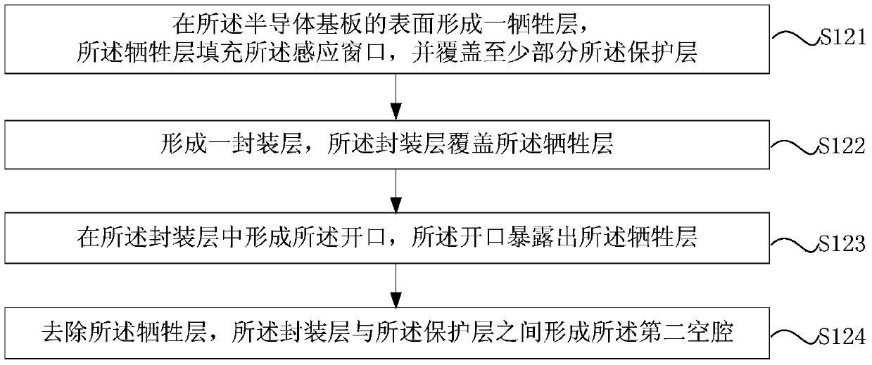
[0032] The semiconductor device of the present invention and its packaging method will be described in more detail below in conjunction with the schematic diagrams, which show the preferred embodiments of the present invention. It should be understood that those skilled in the art can modify the present invention described here and still achieve the advantages of the present invention. Favorable effect. Therefore, the following description should be understood to be widely known to those skilled in the art, and not as a limitation to the present invention.

[0033] For the sake of clarity, not all features of actual embodiments are described. In the following description, well-known functions and structures are not described in detail because they may confuse the present invention due to unnecessary details. It should be considered that in the development of any actual embodiment, a large number of implementation details must be made to achieve the developer's specific goal, suc...


PUM

PropertyMeasurementUnit
thicknessaaaaaaaaaa
thicknessaaaaaaaaaa
thicknessaaaaaaaaaa

Abstract

The invention provides a semiconductor device and an encapsulation method thereof. The semiconductor device comprises a semiconductor substrate, and an encapsulation layer, wherein a first cavity is formed between the surface of partial semiconductor substrate and a sensing layer, a protective layer is formed on the sensing layer, and partial sensing layer exposed from the protective layer is used as a sensing window; the encapsulation layer is arranged on the protective layer, an opening above the first cavity is arranged in the encapsulation layer, and a second cavity is formed between the encapsulation layer and the protective layer. In the semiconductor device provided by the invention, the encapsulation layer is formed on the semiconductor substrate, the encapsulation layer is arranged on the protective layer, the second cavity is formed in front of the protective layer, and the opening in the encapsulation layer is arranged above the first cavity, thereby exposing the sensing window on the first cavity; the indication window can sense the pressure from the external, and the detection on the pressure is realized. The encapsulation layer is directly formed on the semiconductor substrate, the encapsulation of the semiconductor substrate is finished, and the process is simple and convenient.

Description

Technical field [0001] The present invention relates to the technical field of microelectromechanical systems, in particular to a semiconductor device and a packaging method thereof. Background technique [0002] Micro-Electro-Mechanical Systems (MEMS) is a micro-device or system that can be integrated into production, integrating micro-mechanisms, micro-sensors, micro-actuators, and signal processing and control circuits. It is developed with the development of semiconductor integrated circuit micro-processing technology and ultra-precision machining technology. Microelectronic devices using MEMS technology have very broad application prospects in aviation, aerospace, environmental monitoring, biomedicine and almost all fields that people come into contact with. [0003] MEMS sensors have been used in various fields. Due to the needs of the working environment, MEMS sensors must adopt an effective packaging structure and packaging method. The existing packaging method is to manu...

Claims


Application Information

Patent Timeline
Patent Type & Authority Patents(China)
IPC IPC(8): B81C1/00B81B7/00
CPCB81B7/0032B81C1/00261
Inventor 刘孟彬毛剑宏
Owner ZHEJIANG JUEXIN MICROELECTRONICS CO LTD
Features
  • R&D
  • Intellectual Property
  • Life Sciences
  • Materials
  • Tech Scout
  • Unparalleled Data Quality
  • Higher Quality Content
  • 60% Fewer Hallucinations
Learn More