Transistor forming method

A technology of transistors and body regions, which is applied in the direction of semiconductor devices, semiconductor/solid-state device manufacturing, electrical components, etc., can solve the problems that the breakdown voltage of LDMOS transistors needs to be further improved, and achieve size reduction, control capability, and conductance reduction. The effect of on-resistance

Inactive Publication Date: 2017-12-19
SEMICON MFG INT (SHANGHAI) CORP +1
View PDF7 Cites 5 Cited by
  • Summary
  • Abstract
  • Description
  • Claims
  • Application Information

AI Technical Summary

Problems solved by technology

[0006] However, the breakdown voltage of the LDMOS transi

Method used


Image

  • Transistor forming method
  • Transistor forming method
  • Transistor forming method

Examples


Embodiment Construction

[0031] It can be seen from the background art that the breakdown voltage of the LDMOS transistor in the prior art needs to be further improved. The reason for the process analysis problem of forming LDMOS transistors in combination with the existing technology:

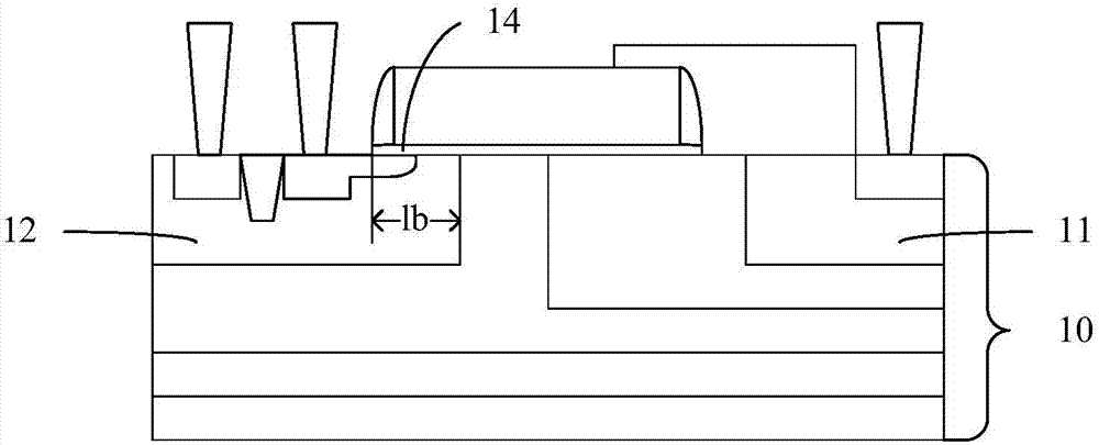
[0032] refer to figure 1 , shows a schematic cross-sectional structure of an LDMOS transistor.

[0033] like figure 1 As shown, the LDMOS transistor includes a substrate 10; an N-type drift region 11 and a P-type body region 12 with a certain interval in the substrate 10; a gate structure 14 on the substrate 10, and the gate structure 14 is located in a part The P-type body region 12 , part of the N-type drift region 11 and the substrate 10 between the P-type body region 12 and the N-type drift region 11 .

[0034] When forming the LDMOS transistor, the gate structure 14 is formed by an etching process after the N-type drift region 11 and the P-type body region 12 . Therefore, in order to ensure that the gate stru...


PUM


Abstract

The invention discloses a transistor forming method. The method comprises steps: a substrate is formed; a gate material layer is formed on the substrate; first etching is carried out on the gate material layer, part of the gate material layer is removed, and part of the substrate is exposed; first ion implantation is carried out on the exposed substrate, a body region with first doping ions is formed in the substrate, and the body region extends below the remaining gate material layer; second etching is carried out on the remaining gate material layer, and the part of the gate material layer at one side away from the body region is removed to form a gate. The gate is formed through twice etching, the first ion implantation to form the body region is carried out between the twice etching, the first ion implantation is directly carried out on the exposed substrate surface, diffusion of ions in the substrate is used to realize extension of the body region towards below the gate, coverage on the body region by the formed gate can be realized for realizing the control capacity of the gate to the body region, the size of an overlapped region between the body region and the gate can also be reduced, and the breakdown voltage of the formed transistor can be further improved.

Description

technical field [0001] The invention relates to the field of semiconductor manufacturing, in particular to a method for forming a transistor. Background technique [0002] A lateral diffusion field effect (Lateral Diffusion MOS, LDMOS) transistor is a semiconductor structure that forms a lateral current path on the surface of a semiconductor substrate through planar diffusion. Compared with traditional MOS transistors, LDMOS transistors have a lightly doped region between the source region and the drain region, which is called a drift region. Therefore, when the LDMOS transistor is connected to a high voltage between the source region and the drain region, the drift region can withstand a higher voltage drop, so the LDMOS transistor can have a higher breakdown voltage. [0003] LDMOS transistors are compatible with complementary metal oxide semiconductor processes, so LDMOS transistors are widely used in power devices. For LDMOS transistors used as power integrated circuit...

Claims


Application Information

Patent Timeline
IPC IPC(8): H01L21/336
CPCH01L29/66689H01L29/66659H01L29/7835H01L29/1045H01L21/26586H01L21/266H01L21/32133H01L21/32139H01L29/66681
Inventor 陈德艳马燕春郑大燮
Owner SEMICON MFG INT (SHANGHAI) CORP
Why Eureka
Try Eureka