PCB antenna

A kind of PCB board and antenna technology, applied in the direction of antenna, resonant antenna, slot antenna, etc., can solve the problem of affecting the 100RF characteristics of the antenna, and achieve the effect of good performance and RF range, less space and vertical height, stable and accurate design

Active Publication Date: 2017-12-29
AXIS
View PDF20 Cites 1 Cited by
  • Summary
  • Abstract
  • Description
  • Claims
  • Application Information

AI Technical Summary

Problems solved by technology

However, the PCB 110 is still an integral part of the anten...

Method used


Image

  • PCB antenna
  • PCB antenna
  • PCB antenna

Examples


Embodiment Construction

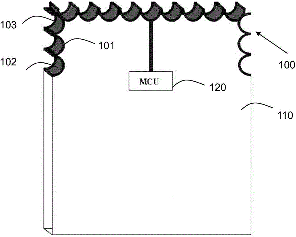
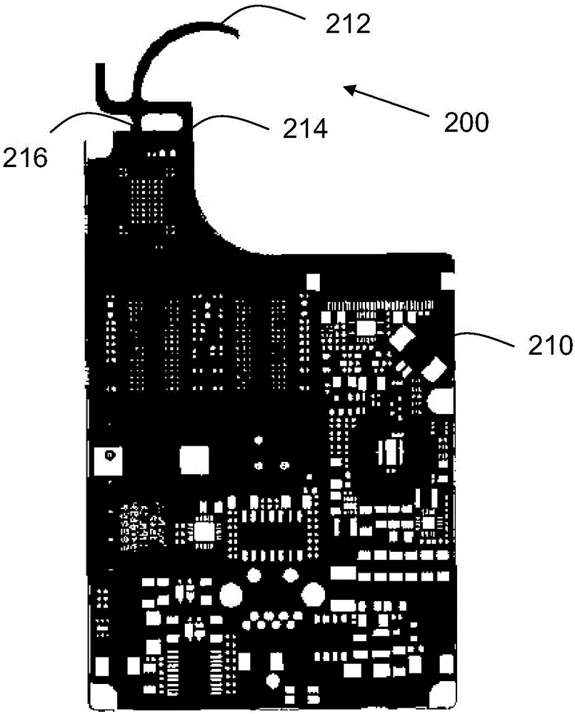
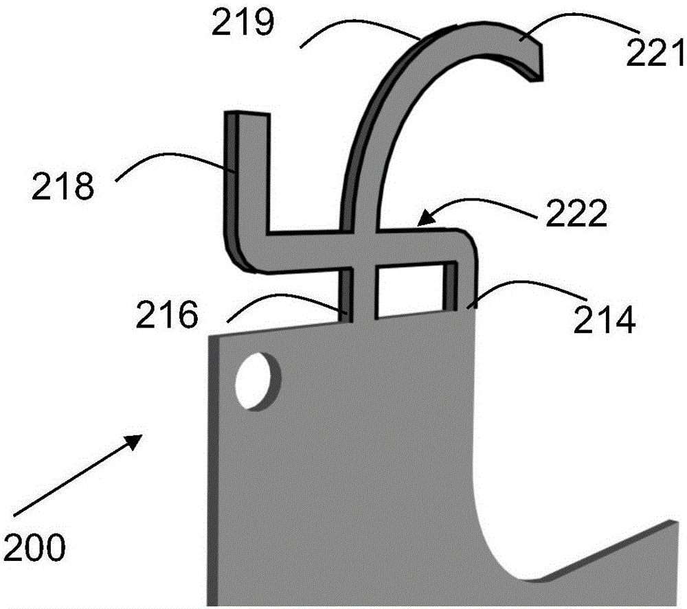
[0024] Figure 2a is a top view of PCB 210 showing one embodiment of PCB antenna 200 . The PCB antenna 200 includes an antenna body 212 integrally formed as part of the PCB 210 . In this example, the antenna 200 is designed as a dual-band antenna for 2.4GHz and 5GHz. The antenna body 212 has an F shape, extending approximately 16 mm from the edge of the remaining PCB and spanning approximately 22 mm. It should be noted that if another design and shape is chosen, the antenna will have other dimensions. The antenna body 212 is cut from the PCB board along most of its perimeter, except for two ends 214 , 216 where it extends from the remainder of the PCB 210 . The antenna body 212 is surrounded or enclosed by metal, eg copper. This can be done through various processes. According to some embodiments herein, antenna body 212 may be surrounded by plating or metallization on the top and bottom layers of PCB 210 , as well as side metallization along the perimeter of antenna body ...


PUM


Abstract

An antenna (200) comprises an antenna body (212). The antenna body is integrally formed as a part of a PCB (210) and the antenna body is enclosed by metal. The antenna body may be enclosed by printed or plated metal on both top and bottom surfaces of the PCB and by edge plated metal along the circumference of the antenna body.

Description

technical field [0001] Embodiments herein relate to antennas arranged on a printed circuit board PCB. In addition, they also refer to the PCB including this antenna, the transceiver and the wireless data acquisition device. Background technique [0002] An antenna is an electronic device that converts electrical energy into radio waves and vice versa. It is typically used with a radio frequency (RF) transceiver that includes a transmitter and receiver. Antennas are an essential element of all devices that use wireless communications. They are used in applications such as radio and television broadcasting, two-way radios, communication receivers, radar, cellular telephones, satellite communications such as the Global Positioning System (GPS), Wireless Speaker and Audio (WISA) systems, Zigbee or Z-Wave systems and wireless local area networks ( WLAN), and other wireless communication devices such as wireless microphones, Bluetooth-enabled devices, wireless computer networks...

Claims


Application Information

Patent Timeline
IPC IPC(8): H01Q1/22H01Q1/38
CPCH01Q1/22H01Q1/38H01Q1/2291H01Q1/48H01Q9/42H01Q5/371H01Q9/0407H01Q13/10H01Q5/30H01Q5/40
Inventor H·霍夫莫勒
Owner AXIS
Why Eureka
Try Eureka