Compression type semiconductor device
A semiconductor, pressure-bonding technology, applied in the direction of semiconductor devices, semiconductor/solid-state device manufacturing, semiconductor/solid-state device components, etc., can solve the problem that pressure-bonding semiconductor devices cannot be converted, and achieve high reliability.
- Summary
- Abstract
- Description
- Claims
- Application Information
AI Technical Summary
Problems solved by technology
Method used
Image
Examples
Embodiment approach 1
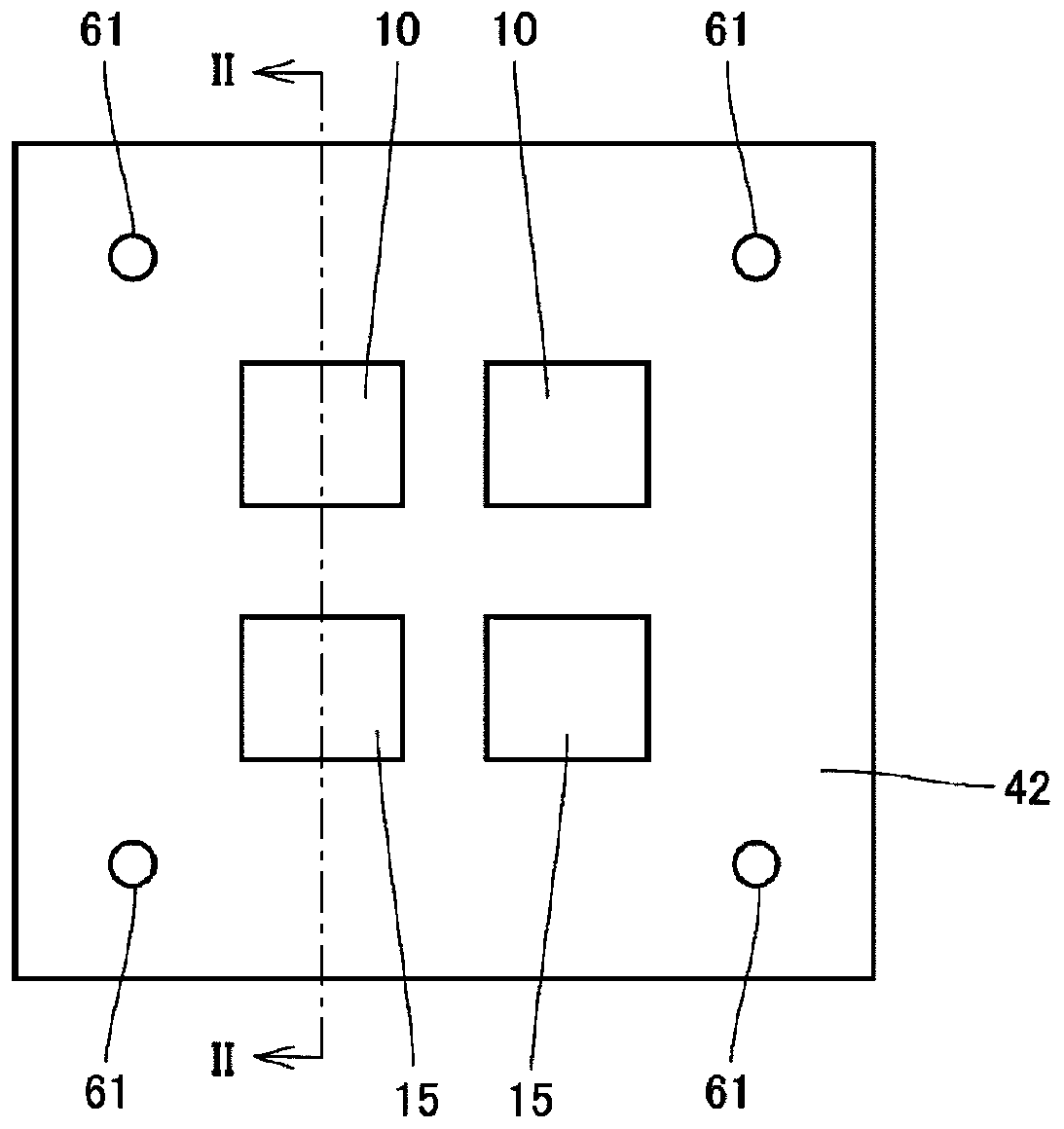
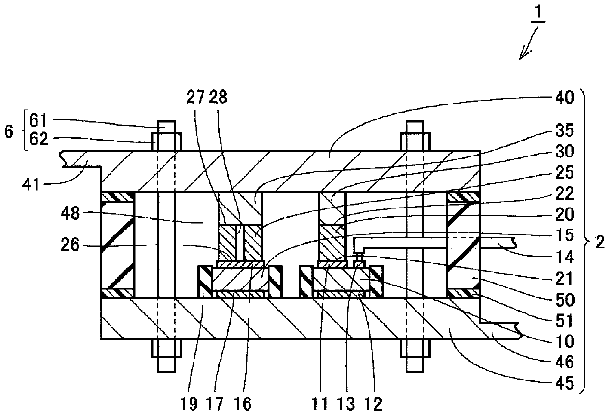
[0044] refer to Figure 1 to Figure 7 , the pressure-bond type semiconductor device 1 according to Embodiment 1 will be described. The pressure-bonding semiconductor device 1 of the present embodiment includes a pressure-bonding semiconductor element 2 and a pressing portion 6 .
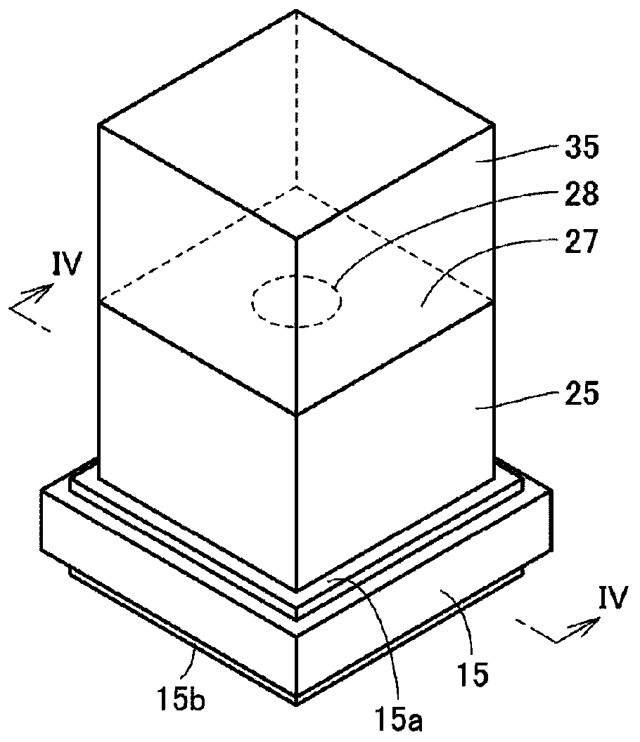
[0045] The pressure-bonding semiconductor element 2 mainly includes a first semiconductor chip 10 , a second semiconductor chip 15 , a first common electrode plate 40 , a first intermediate electrode 20 , a second intermediate electrode 25 , a second common electrode plate 45 and a barrel 50 . The crimp-type semiconductor element 2 may further include a first connection member 30 and a second connection member 35 .
[0046] The first semiconductor chip 10 is a three-terminal type semiconductor element. The first semiconductor chip 10 may also be a semiconductor switching element. Examples of the semiconductor switching element include transistors such as insulated gate bipolar transistors (IGBTs) ...
Embodiment approach 2
[0066] refer to Figure 8 , the pressure-bond type semiconductor device 1a of Embodiment 2 will be described. The pressure-bond semiconductor device 1 a of the present embodiment basically has the same configuration as the pressure-bond semiconductor device 1 of Embodiment 1, but mainly differs in the following points.
[0067] The pressure-bond semiconductor device 1 a of the present embodiment includes a pressure-bond semiconductor element 2 a. The crimp-type semiconductor element 2a of this embodiment does not include the first connecting member 30 and the second connecting member 35 (see figure 2 ). The first common electrode plate 40 and the second semiconductor chip 15 close one or more second through holes 28 . Specifically, the first common electrode plate 40 and the fourth electrode 16 of the second semiconductor chip 15 close one or more second through holes 28 .
[0068] Effects of the pressure-bond type semiconductor device 1a of this embodiment will be descri...
Embodiment approach 3
[0072] refer to Figure 9 to Figure 12 , the pressure-bond type semiconductor device 1b of Embodiment 3 will be described. The pressure-bond semiconductor device 1 b of the present embodiment basically has the same configuration as the pressure-bond semiconductor device 1 of Embodiment 1, but mainly differs in the following points.
[0073] The pressure-bond semiconductor device 1b of this embodiment includes a pressure-bond semiconductor element 2b. The pressure-bond semiconductor element 2b of this embodiment includes a first intermediate electrode 20b. The first intermediate electrode 20 b has one or more first through holes 23 penetrating between the first surface 21 and the second surface 22 . Such as Figure 9 as well as Figure 10 As shown, in this embodiment, the first intermediate electrode 20 b may have one first through hole 23 . Such as Figure 12 As shown, in a modified example of this embodiment, the first intermediate electrode 20b may have a plurality of ...
PUM
 Abstract
Description
Claims
Application Information


