Method for preparing micro-nano scale periodic or non-periodic structure at material surface
A periodic structure and non-periodic technology, applied in the manufacture of microstructure devices, microstructure technology, microstructure devices, etc., can solve problems such as lattice mismatch and thermal stress mismatch, and achieve low noise and operability Strong, long product life cycle effect
- Summary
- Abstract
- Description
- Claims
- Application Information
AI Technical Summary
Problems solved by technology
Method used
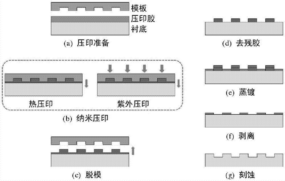
Image

Examples
Embodiment 1
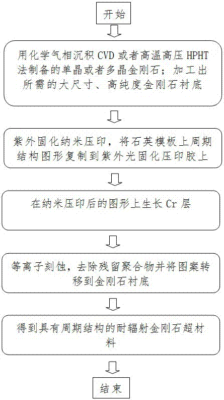
[0031] High-purity single-crystal diamond was prepared by microwave plasma chemical vapor deposition equipment with a power of 75KW, and its size was processed into a high-purity diamond substrate of 20mm×20mm×10mm. A matrix-shaped periodic pattern with a resolution of 10nm was produced by etching technology and other steps. The surface of the obtained sample was smooth and straight, and the bottom of the etching groove was close to a square. This periodic diamond metamaterial can be used to prepare various reflection and transmission gratings, photonic crystal light-emitting diodes, Fresnel lenses, etc. under high radiation conditions, and can be used in medical treatment, outer space, nuclear power plants, etc. On the detection device used in the place.
Embodiment 2
[0033] High-purity single crystal diamond was prepared by microwave plasma chemical vapor deposition equipment with a power of 75KW, and its size was processed into a high-purity diamond substrate of 20mm×20mm×6mm. A 5nm matrix-shaped periodic pattern was produced by etching technology and other steps. The surface of the obtained sample was smooth, with good steepness, and the bottom of the etching groove was close to a square. This periodic diamond metamaterial can be used to prepare various reflection and transmission gratings, photonic crystal light-emitting diodes, Fresnel lenses, etc. under high radiation conditions, and can be used in medical treatment, outer space, nuclear power plants, etc. On the detection device used in the place.
Embodiment 3
[0035] High-purity single crystal diamond was prepared by microwave plasma chemical vapor deposition equipment with a power of 75KW, and its size was processed into a high-purity diamond substrate of 20mm×20mm×6mm. A 50nm inverted V-shaped periodic pattern was produced by etching technology. The surface of the obtained sample was smooth, with good steepness, and the bottom of the etching groove was close to square. This periodic diamond metamaterial can be used to prepare various reflection and transmission gratings, photonic crystal light-emitting diodes, Fresnel lenses, etc. under high radiation conditions, and can be used in medical treatment, outer space, nuclear power plants, etc. On the detection device used in the place.
PUM
| Property | Measurement | Unit |
|---|---|---|
| Thickness | aaaaa | aaaaa |
Abstract
Description
Claims
Application Information
 - R&D Engineer
- R&D Manager
- IP Professional
- Industry Leading Data Capabilities
- Powerful AI technology
- Patent DNA Extraction
Browse by: Latest US Patents, China's latest patents, Technical Efficacy Thesaurus, Application Domain, Technology Topic.
© 2024 PatSnap. All rights reserved.Legal|Privacy policy|Modern Slavery Act Transparency Statement|Sitemap