Anti-fouling substrate and preparation method thereof

A substrate and anti-fouling technology, applied in semiconductor/solid-state device manufacturing, electrical components, electrical solid-state devices, etc., can solve the problems of poor sample surface wear resistance, difficulty in maintaining the original appearance of the sample surface, and poor surface wear resistance. Solve the effect of poor surface wear resistance, precise and controllable size, and improved wear resistance

Inactive Publication Date: 2018-01-09
CHAOZHOU THREE CIRCLE GRP
View PDF4 Cites 6 Cited by
  • Summary
  • Abstract
  • Description
  • Claims
  • Application Information

AI Technical Summary

Problems solved by technology

[0003] In order to make the samples have anti-fouling function, superhydrophobic coatings are mostly prepared on the surface of the samples, but the samples prepared in this way have the problem of poor surface wear resistance, and it is difficult to maintain the original shape of the sample surface after repeated friction
In order to make the surface of the sample wear-resistant, in the traditional preparation process, the convex array is usually implanted on the surface of the substrate through a specific process, and the convex array forms an interface bond with the substrate. After repeated friction, the convex array is easily removed from the substrate. Surface peeling, which easily leads to poor wear resistance of the sample surface

Method used


Image

  • Anti-fouling substrate and preparation method thereof
  • Anti-fouling substrate and preparation method thereof
  • Anti-fouling substrate and preparation method thereof

Examples


preparation example Construction

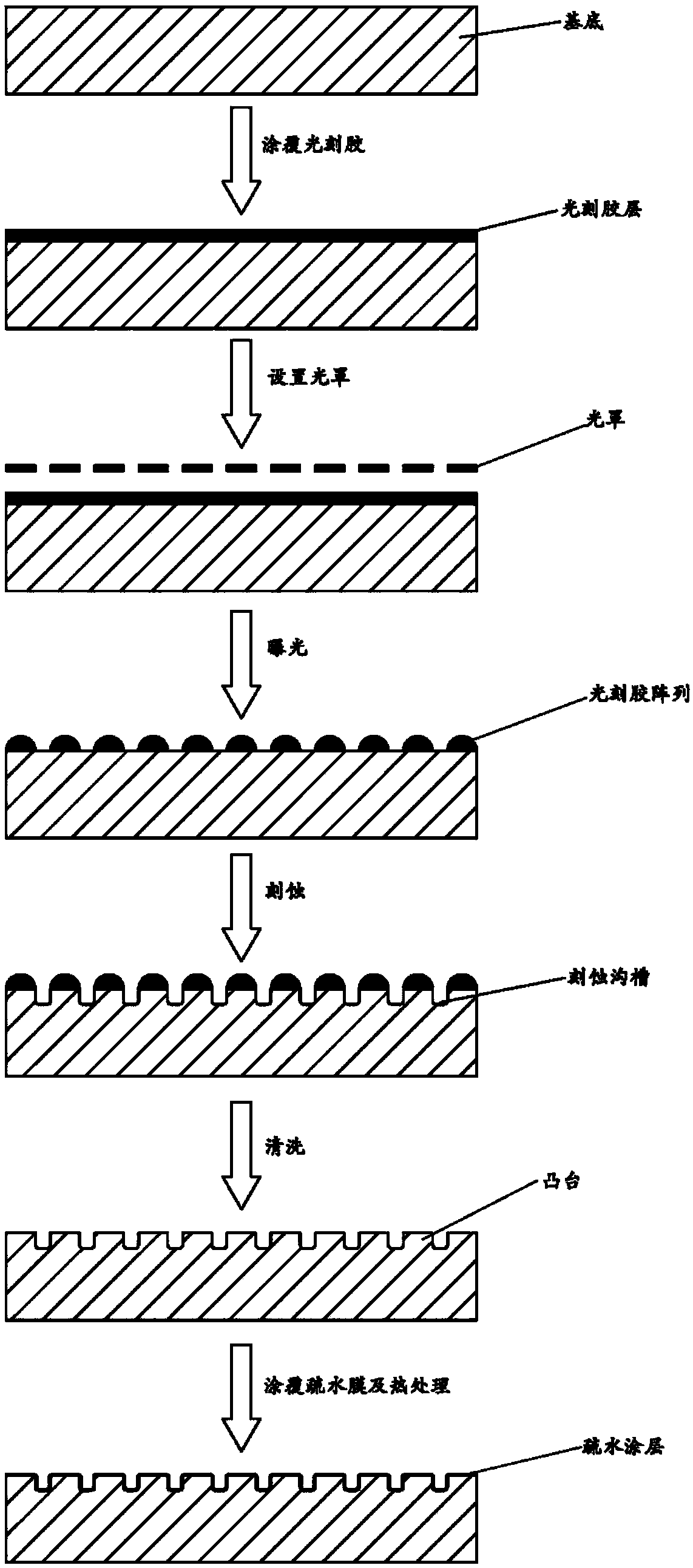
[0043] attached figure 1 It is a flowchart of an embodiment of the preparation method of the anti-fouling substrate of the present invention, specifically, the preparation method of the anti-fouling substrate of the present invention includes the following steps:

[0044] (1), coating a layer of photoresist on the surface of the zirconia substrate;

[0045] (2), the base that step (1) gained is coated with photoresist carries out deep ultraviolet exposure treatment under different photomasks, forms photoresist array;

[0046] (3), etch the base template after the exposure treatment obtained in step (2), and then clean the etched base template to obtain a base with a boss;

[0047] (4), coating the substrate with bosses obtained in step (3) with a hydrophobic material;

[0048] (5) Heat-treating the substrate coated with the hydrophobic material to obtain the antifouling substrate.

Embodiment 1

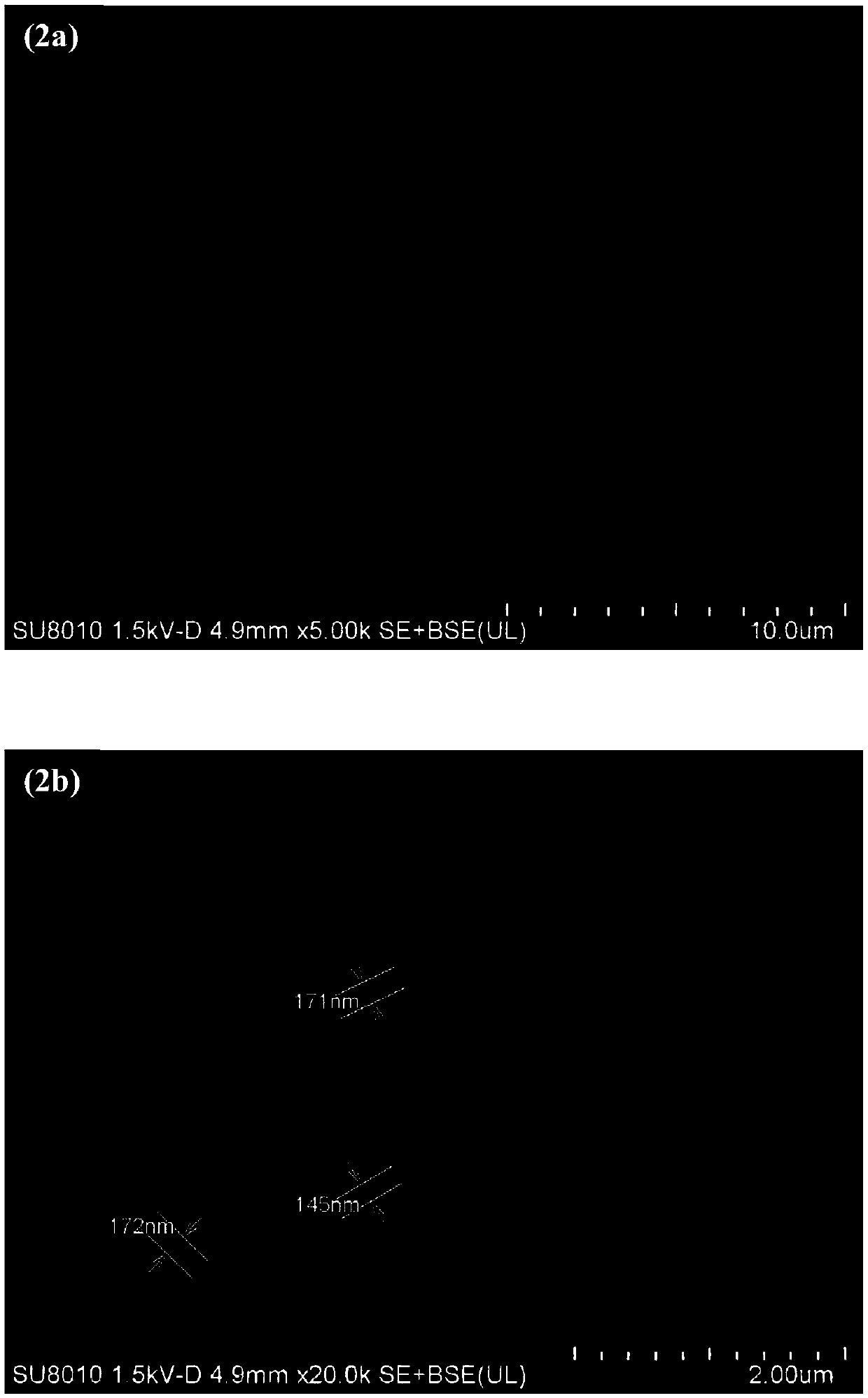
[0051] An embodiment of the antifouling substrate of the present invention, the base material of the antifouling substrate is zirconia, the coating is perfluorodecyltriethoxysilane, the average height of the bosses is 120nm, each The average upper surface area of ​​the boss is 1.767×10 4 nm 2 , the average spacing between adjacent bosses is 150nm.

[0052] The preparation method of the antifouling substrate described in this embodiment comprises the following steps:

[0053] (1), clean the zirconia substrate with a cleaning agent, then clean it with ultrasonic waves for 5 minutes, and then clean it with deionized water for 2 minutes;

[0054] (2) Coating the photoresist on the zirconia substrate by spin coating with a coating thickness of 0.8 μm, and then baking at 100° C. for 1 min;

[0055] (3), the substrate coated with photoresist obtained in step (2) is subjected to exposure treatment using a grating;

[0056] (4), adopt reactive ion etching to the substrate of step (...

Embodiment 2

[0060] An embodiment of the antifouling substrate of the present invention, the base material of the antifouling substrate is zirconia, the coating is perfluorodecyltriethoxysilane, the average height of the bosses is 120nm, each The average upper surface area of ​​the boss is 1.767×10 4 nm 2 , the average spacing between adjacent bosses is 150nm.

[0061] The preparation method of the antifouling substrate described in this embodiment comprises the following steps:

[0062] (1), clean the zirconia substrate with a cleaning agent, then clean it with ultrasonic waves for 5 minutes, and then clean it with deionized water for 2 minutes;

[0063] (2) Coating the photoresist on the zirconia substrate by spin coating with a coating thickness of 0.8 μm, and then baking at 100° C. for 1 min;

[0064] (3), the substrate coated with photoresist obtained in step (2) is exposed to deep ultraviolet light, the photomask is a circular array with a period of 150nm, and exposed to deep ultr...


PUM

PropertyMeasurementUnit
heightaaaaaaaaaa
thicknessaaaaaaaaaa
thicknessaaaaaaaaaa

Abstract

The invention discloses an anti-fouling substrate, which comprises a substrate. The surface of the substrate at least has one function region. At least a part of the function region has a coating layer. The function region has a plurality of bumps. The average height of the bumps is 10-2000 nm; the average upper surface area of the bumps is 78-1.964*10<5> nm<2>; and the average interval between adjacent two bumps is 7-5000 nm. The coating layer is made of a hydrophobic material. The invention also discloses a preparation method of the anti-fouling substrate. The prepared anti-fouling substratehas higher anti-fouling performance and abrasion resistance, and the substrate has multiple choices; the anti-fouling substrate can realize etching on the substrate surface directly, so that the problem of poor surface abrasion resistance can be solved; meanwhile, by controlling surface etching depth, sample surface appearance can be controlled; and the preparation method of the anti-fouling substrate is low in production cost, simple in process and can realize large-scale batch production.

Description

technical field [0001] The invention relates to an antifouling material, in particular to an antifouling substrate and a preparation method thereof. Background technique [0002] The surface of the antifouling material generally has a hydrophobic surface, and the hydrophobic surface generally refers to a surface whose contact angle between a solid surface and water is greater than 120°. Since the contact area between the hydrophobic surface and the water droplet is very small, the water droplet rolls off the surface very easily. Therefore, the hydrophobic surface not only has the function of self-cleaning, but also has the functions of anti-current conduction, anti-corrosion, waterproof, anti-fog, anti-virus, anti-snow, anti-frost, anti-adhesion, anti-pollution, etc. It has broad application prospects in fields such as biomedicine, daily necessities and packaging, transportation tools, and microanalysis. [0003] In order to make the samples have anti-fouling function, sup...

Claims


Application Information

Patent Timeline
Patent Type & Authority Applications(China)
IPC IPC(8): H01L23/13H01L23/14H01L21/02H01L21/027
Inventor 邱基华
Owner CHAOZHOU THREE CIRCLE GRP
Why Eureka
Try Eureka