ldmos device with esd protection function and its layout

An ESD protection and device technology, applied in the direction of semiconductor devices, electrical solid devices, electrical components, etc., can solve problems such as false opening, poor electrostatic discharge capability, device or chip burnout, etc., to avoid latch-up effect, improve holding voltage, The effect of high electrostatic discharge capability

Active Publication Date: 2020-03-13
SEMICON MFG INT TIANJIN +1
View PDF3 Cites 0 Cited by
  • Summary
  • Abstract
  • Description
  • Claims
  • Application Information

AI Technical Summary

Problems solved by technology

Generally speaking, an LDMOS device is a kind of high-voltage transistor, which itself has a high breakdown voltage, but when it enters a snapback collapse state, its holding voltage (holding voltage) Vh and corresponding holding current (holding current) Ih is relatively low, so when the LDMOS device is used as an electrostatic discharge (Electro Static discharge, ESD) protection device, its electrostatic discharge capability is poor, and it is prone to parasitic latch (Latch up) effect or false opening, causing the device or chip to burn

Method used


Image

  • ldmos device with esd protection function and its layout
  • ldmos device with esd protection function and its layout
  • ldmos device with esd protection function and its layout

Examples


Embodiment 1

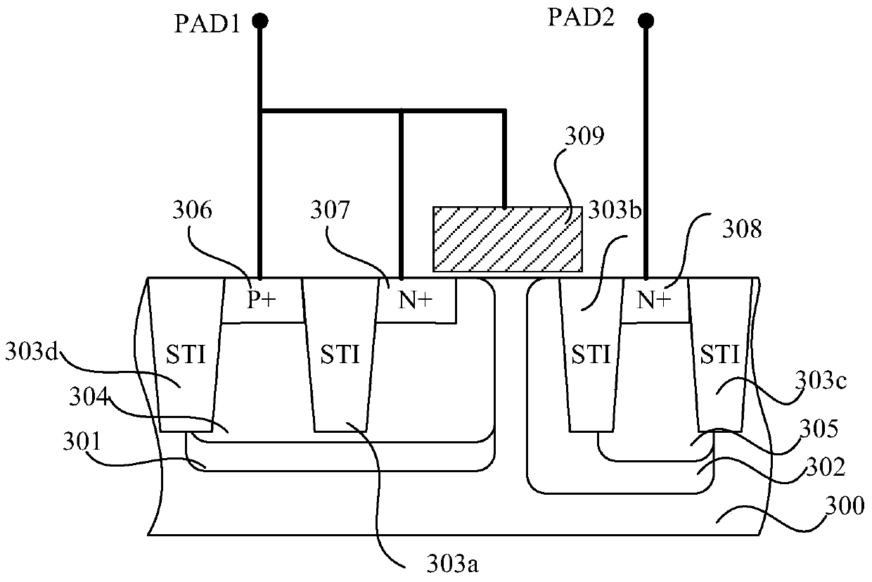
[0032] Please refer to Figure 3A The present invention proposes an LDMOS device with ESD protection function, comprising a P-type substrate 300 with a first deep P well 301 and a deep N well 302 arranged laterally; the surface of the first deep P well 301 is laterally arranged with The first P+ implant region 306 and the first N+ implant region 307, the first P+ implant region 306 and the first N+ implant region 307 are isolated by the first isolation structure 303a, and the first N+ implant region 307 is used as the LDMOS device The first source region (source); the surface of the deep N well 302 is provided with a second N+ implantation region 308, and the second N+ implantation region 308 is used as the drain region (drain) of the LDMOS device, passing through the first N+ implantation region 307 The second isolation structure 303b is isolated. Wherein, a first P well implantation region 304 having a shallower depth than the first deep P well 301 is provided in the first ...

Embodiment 2

[0052] Please refer to Figure 3B , the present embodiment provides an LDMOS device with ESD protection function, including a P-type substrate 300 provided with a first deep P well 301a, a deep N well 302 and a second deep P well 301b in sequence along the lateral direction; the first A first P+ implantation region 306a and a first N+ implantation region 307a are arranged laterally on the surface of the deep P well 301a, and the first P+ implantation region 306a and the first N+ implantation region 307a are separated by a first isolation structure 303a, and the first An N+ implantation region 307a is used as the first source region (source) of the LDMOS device; the surface of the deep N well 302 is provided with a second N+ implantation region 308, and the second N+ implantation region 308 is used as the drain region (drain) of the LDMOS device, and The first N+ implantation region 307a is isolated by the third isolation structure 303b, the surface of the second deep P well 30...


PUM


Abstract

The invention provides an LDMOS device with an ESD protection function and a layout of the LDMOS device. A deep N well of a drain region of the LDMOS device is additionally provided with a shallower Nwell injection region, and a deep P well of a source region of the LDMOS device is additionally provided with a shallower P well injection region, thereby greatly increasing the holding voltage and corresponding holding current of the LDMOS device, and avoiding the latch-up effect more effectively. Therefore, an ESD current can be released before the LDMOS device enters a snapback state, so the LDMOS device is stronger in electrostatic discharge capability. According to the layout of the LDMOS device, an N well injection region is added above the layout of the drain region, and a P well injection region is added above the layout of the source region. The ion implantation in the deep P well, the deep N well, the N well injection region and the P well injection region can be achieved without an additional mask template. The LDMOS device can be technologically compatible with the conventional CMOS BCD technology in the industry.

Description

technical field [0001] The invention relates to the technical field of electrostatic discharge protection design of integrated circuits, in particular to an LDMOS device with ESD protection function and its layout. Background technique [0002] Lateral Diffused Metal-Oxide-Semiconductor (LDMOS) devices have been widely used in many types of applications, such as high voltage semiconductor device applications. Generally speaking, an LDMOS device is a kind of high-voltage transistor, which itself has a high breakdown voltage, but when it enters a snapback collapse state, its holding voltage (holding voltage) Vh and corresponding holding current (holding current) Ih is relatively low, so when the LDMOS device is used as an electrostatic discharge (Electro Static discharge, ESD) protection device, its electrostatic discharge capability is poor, and it is prone to parasitic latch (Latch up) effect or false opening, causing the device or chip to burn. [0003] Therefore, there i...

Claims


Application Information

Patent Timeline
Patent Type & Authority Patents(China)
IPC IPC(8): H01L27/02H01L29/78
Inventor 李宏伟陈光雷玮
Owner SEMICON MFG INT TIANJIN
Why Eureka
Try Eureka