Optical switch
An optical switch and optical crystal technology, applied in the field of optical switches, can solve the problems of increased power consumption and slow speed, and achieve the effects of improving sensitivity, improving response characteristics and reducing driving voltage.
- Summary
- Abstract
- Description
- Claims
- Application Information
AI Technical Summary
Problems solved by technology
Method used
Image
Examples
no. 1 approach
[0052] (optical switch C)
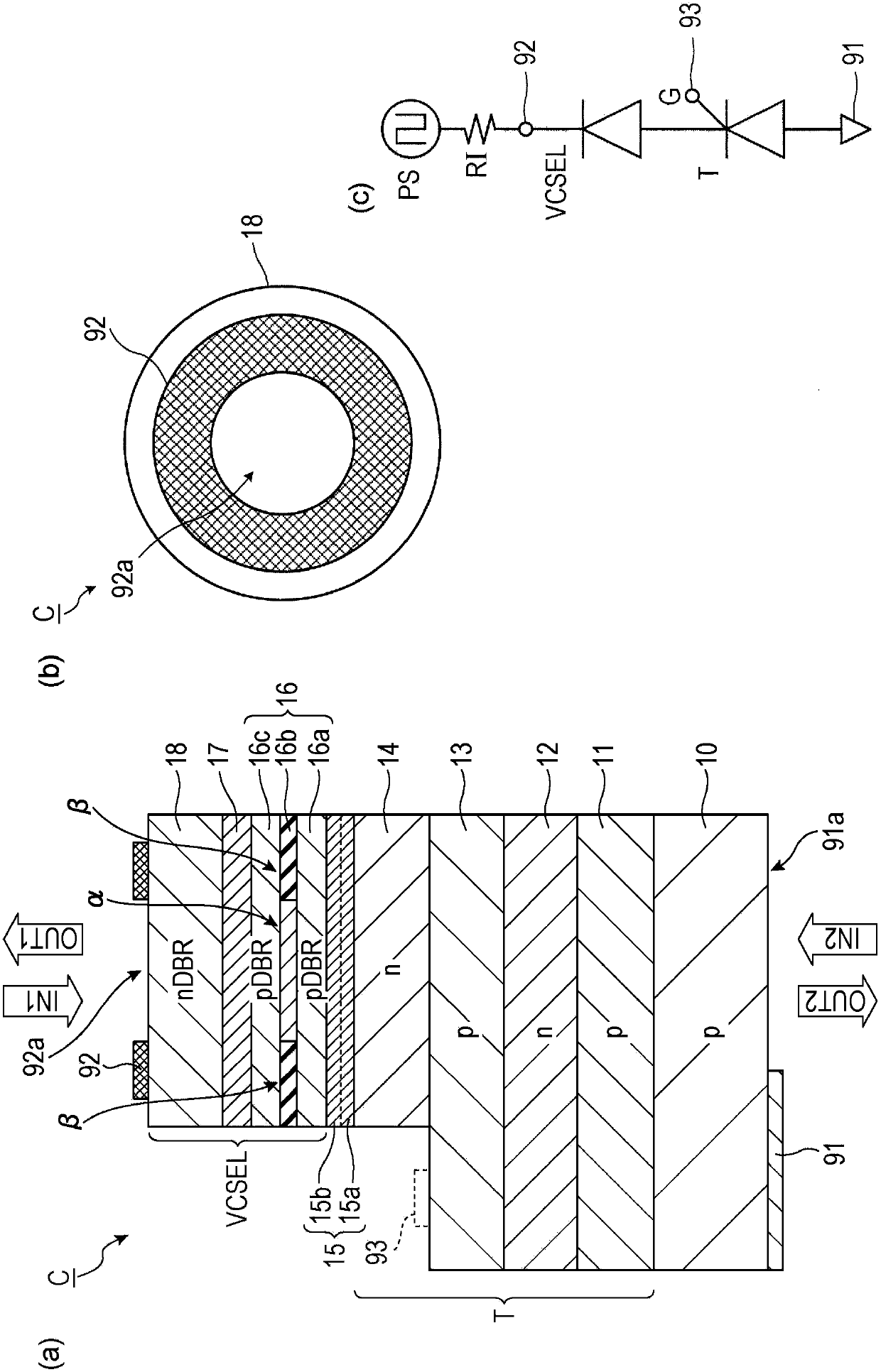
[0053] figure 1 It is a figure explaining the optical switch C of 1st Embodiment. figure 1 (a) is a sectional view, figure 1 (b) is a plan view, figure 1 (c) is an equivalent circuit.
[0054] The optical switch C described here is a photothyristor T turned on by the input of an optical signal (incident light), and a light emitting element (here, as an example, vertical The cavity surface emitting laser VCSEL (Vertical Cavity Surface Emitting Laser)) is composed of a combination.
[0055] The optical switch C is configured, for example, as an integrated circuit (IC) chip formed of compound semiconductor layers such as GaAs, GaAlAs, and AlAs stacked monolithically (epitaxially) on a substrate 10 such as GaAs.
[0056] pass figure 1 (a) The cross-sectional structure of the optical switch C is illustrated.
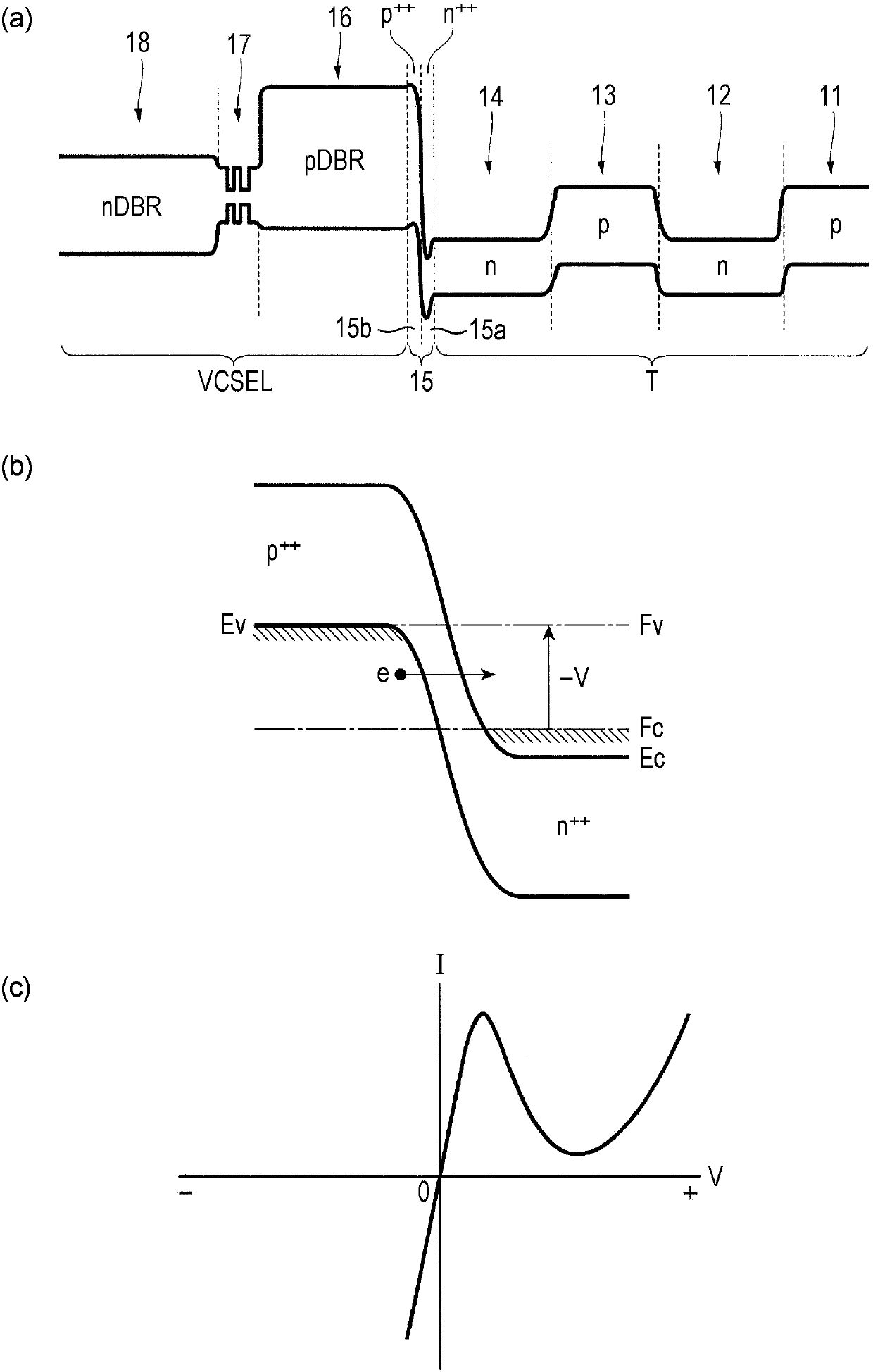
[0057] In the optical switch C, the photothyristor T and the vertical cavity surface emitting laser VCSEL are laminated and electrically co...
no. 2 approach
[0233] Figure 12 It is a figure explaining the optical switch C of 2nd Embodiment. Figure 12 (a) is a sectional view, Figure 12 (b) is a plan view, Figure 12 (c) is an equivalent circuit.
[0234] In the optical switch C of the second embodiment, a DBR layer (p anode (DBR) layer 16 ) functioning as an anode of a vertical cavity surface emitting laser VCSEL, a light emitting layer 17 , and The cathode of the vertical cavity surface emitting laser VCSEL functions as the DBR layer (n-cathode (DBR) layer 18 ).
[0235] Furthermore, a tunnel junction (tunnel diode) layer 15 is provided on the n cathode (DBR) layer 18 . The tunnel junction layer 15 is made of n-type impurity (dopant) added (doped) at a high concentration. ++ layer 15a and the p-type impurity doped at high concentration ++ layer 15b.
[0236] Furthermore, on the tunnel junction layer 15, a p-type anode layer 11 (p anode layer 11) functioning as an anode of the photothyristor T, and an n-type gate layer 12 ...
no. 3 approach
[0254] Figure 13 It is a figure explaining the optical switch C of 3rd Embodiment. Figure 13 (a) is a sectional view, Figure 13 (b) is a plan view. Equivalent circuit with Figure 12 The optical switch C of the second embodiment shown in (c) is the same, so description is omitted.
[0255] The optical switch C of the third embodiment includes an opening 20 dug in the center of the photothyristor T. As shown in FIG. The opening 20 has a circular cross-sectional shape and is provided from the surface of the photothyristor T toward the vertical cavity surface emitting laser VCSEL. Furthermore, the cathode electrode 92 is provided in an annular shape on the n-cathode layer 14 so as to surround the opening 20 .
[0256] In addition, the cross-sectional shape of the opening 20 may not be circular, and the shape of the cathode electrode 92 may not be circular.
[0257] In addition, although the opening part 20 is provided so that the center part of the photothyristor T may b...
PUM
 Abstract
Description
Claims
Application Information
 - R&D
- Intellectual Property
- Life Sciences
- Materials
- Tech Scout
- Unparalleled Data Quality
- Higher Quality Content
- 60% Fewer Hallucinations
Browse by: Latest US Patents, China's latest patents, Technical Efficacy Thesaurus, Application Domain, Technology Topic, Popular Technical Reports.
© 2025 PatSnap. All rights reserved.Legal|Privacy policy|Modern Slavery Act Transparency Statement|Sitemap|About US| Contact US: help@patsnap.com


