Indium phosphate bismuth material and preparation method thereof, laser using indium phosphate bismuth material and production method of laser

A technology of indium phosphobismuth and indium phosphobismuth, which is applied in the field of materials science, can solve the problems of narrow band gap, limit, and inability to improve semiconductor performance, and achieve good semiconductor performance, increase spin-orbit splitting, and suppress Russian Intermittent compounding effect

Active Publication Date: 2018-01-09
CHAOJING TECH BEIJING CO LTD
View PDF5 Cites 1 Cited by
  • Summary
  • Abstract
  • Description
  • Claims
  • Application Information

AI Technical Summary

Problems solved by technology

However, indium phosphide also has the following defects: although its band gap is very narrow, it is also limited.
That is to say, the band gap of indium phosphide cannot continue to narrow after being narrowed to a certain extent, nor can it continue to improve its semiconductor performance.

Method used


Image

  • Indium phosphate bismuth material and preparation method thereof, laser using indium phosphate bismuth material and production method of laser
  • Indium phosphate bismuth material and preparation method thereof, laser using indium phosphate bismuth material and production method of laser
  • Indium phosphate bismuth material and preparation method thereof, laser using indium phosphate bismuth material and production method of laser

Examples


Embodiment Construction

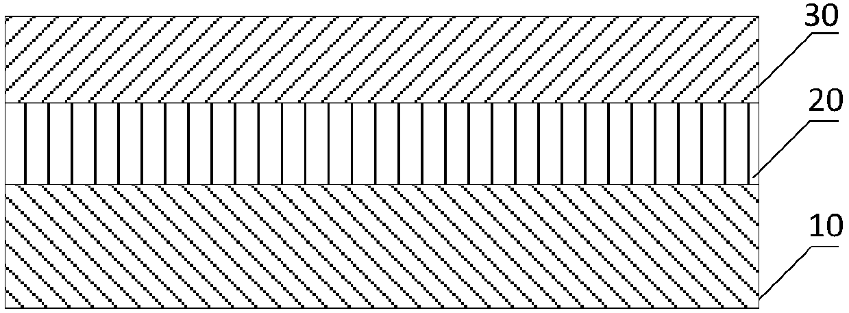
[0048] Please refer to figure 1 , in this embodiment, the indium phosphide bismuth material includes: an indium phosphide substrate 10 , an indium phosphide buffer layer 20 and an indium phosphide bismuth body 30 . Wherein the indium phosphide buffer layer 20 is disposed on the indium phosphide substrate. The indium phosphide bismuth body 30 is disposed on the indium phosphide buffer layer 20 . The chemical formula of indium phosphobismuth bulk is InP 1-x Bi x , where x is the concentration percentage of bismuth atoms, and 0

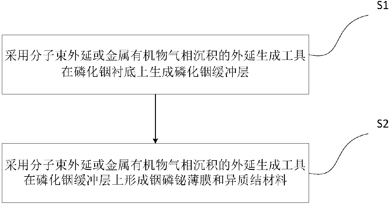
[0049] Please refer to figure 2 , in this embodiment, the preparation method of indium phosphide bismuth material comprises the following steps:

[0050] S1: An indium phosphide buffer layer is formed on an indium phosphide substrate by molecular beam epitaxy or metal-organic vapor deposition.

[0051] S2: Form an indiu...


PUM

PropertyMeasurementUnit
thicknessaaaaaaaaaa
thicknessaaaaaaaaaa
thicknessaaaaaaaaaa

Abstract

The invention relates to the field of materials science, in particular to an indium phosphide bismuth material and a preparation method thereof, and a laser using the material and a preparation method thereof. The indium phosphide bismuth material comprises: an indium phosphide substrate; an indium phosphide buffer layer, disposed on the indium phosphide substrate; and an indium phosphide bismuth body disposed on the indium phosphide buffer layer; the chemical formula of the indium phosphide bismuth body is InP1-xBix, wherein x is the concentration of bismuth atoms percentage, and 0

Description

technical field [0001] The invention relates to the field of material science, in particular to an indium phosphide bismuth material. Background technique [0002] III-V semiconductor materials are widely used in the fields of lasers, photoelectric tubes and optical fiber communications. Among them, narrow bandgap materials have great advantages in the fields of microelectronics and optoelectronics as substrates for high-speed electronics and optoelectronic devices, and are also very suitable for vertical optical field lasers and high electron carrier transistors. Taking indium phosphide as an example, it has a narrow band gap and high semiconductor performance. However, indium phosphide also has the following disadvantages: although its band gap is very narrow, it also has a limit. That is, the band gap of indium phosphide cannot continue to be narrowed after being narrowed to a certain extent, nor can it continue to improve its semiconductor performance. Contents of th...

Claims


Application Information

Patent Timeline
Patent Type & Authority Applications(China)
IPC IPC(8): H01S5/30
Inventor 梁丹王庶民张丽
Owner CHAOJING TECH BEIJING CO LTD
Why Eureka
Try Eureka