

Display panel, manufacture method thereof and display device
A technology for a display panel and a manufacturing method, which is applied in the manufacture of semiconductor/solid-state devices, semiconductor devices, electrical components, etc., can solve the problems of unfavorable narrow borders and the width of the left and right borders of the display panel, so as to reduce the border area and reduce the layout area. , Conducive to the effect of narrow border
- Summary
- Abstract
- Description
- Claims
- Application Information
AI Technical Summary
Problems solved by technology
Method used
Image

Examples
Embodiment Construction
[0025] The application will be further described in detail below in conjunction with the accompanying drawings and embodiments. It should be understood that the specific embodiments described here are only used to explain related inventions, rather than to limit the invention. It should also be noted that, for ease of description, only parts related to the invention are shown in the drawings.
[0026] It should be noted that, in the case of no conflict, the embodiments in the present application and the features in the embodiments can be combined with each other. The present application will be described in detail below with reference to the accompanying drawings and embodiments.
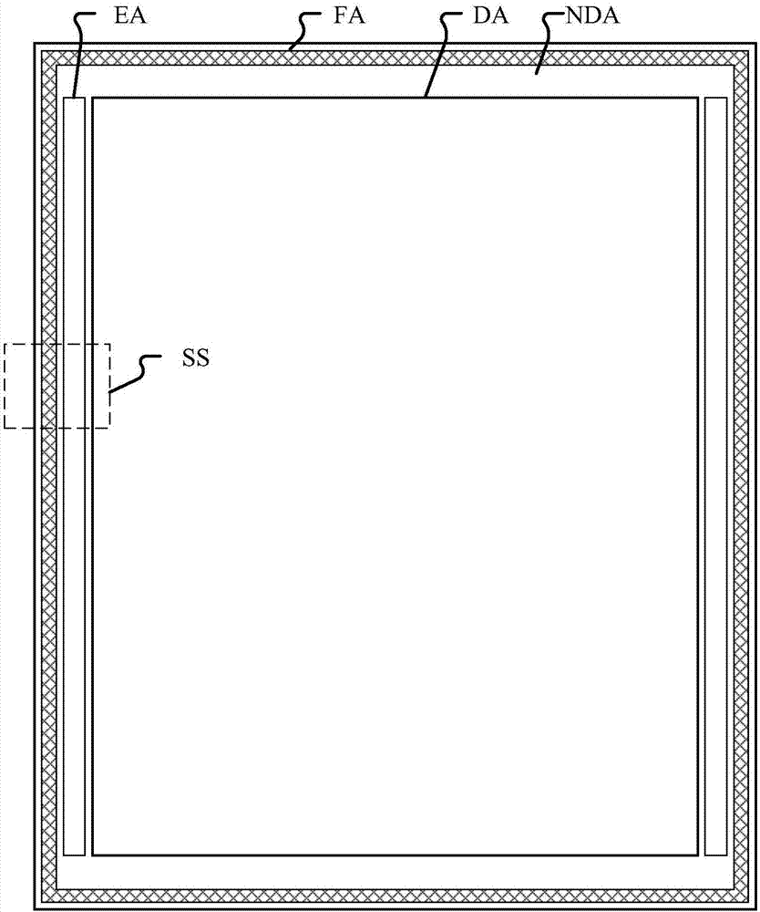
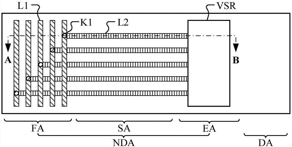
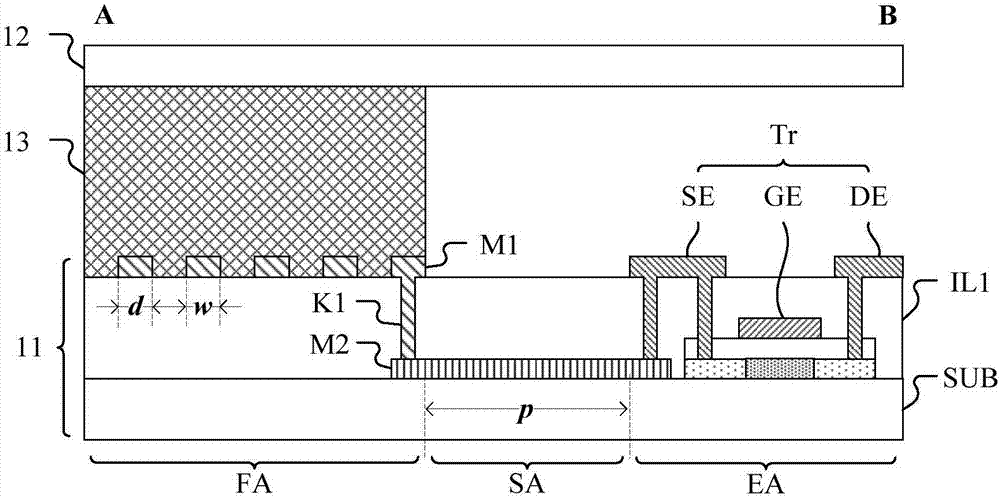
[0027] Figure 1A A schematic diagram showing a display panel according to an embodiment of the present application, Figure 1B show Figure 1A An enlarged schematic diagram of the middle region SS, Figure 1C for along Figure 1B Cross-sectional view of line AB in.
[0028] Such as Figure 1A...
PUM
| Property | Measurement | Unit |
|---|---|---|
| Line width | aaaaa | aaaaa |
| Minimum spacing | aaaaa | aaaaa |
Abstract
Description
Claims
Application Information