Check patentability & draft patents in minutes with Patsnap Eureka AI!

A fin field-effect transistor and a manufacturing method thereof

A technology of field effect transistors and manufacturing methods, which is applied in the field of fin field effect transistors, can solve the problems of small size, difficult application of fin field effect transistors, and inability of fin field effect transistors to withstand excessive voltage, so as to avoid crossover pressure effect

Inactive Publication Date: 2018-01-12
REALTEK SEMICON CORP
View PDF4 Cites 0 Cited by
  • Summary
  • Abstract
  • Description
  • Claims
  • Application Information

AI Technical Summary

Problems solved by technology

[0003] However, due to the small size, FinFETs cannot withstand excessive voltage at the semiconductor channel, making it difficult for FinFETs to be used in high-voltage environments

Method used


Image

  • A fin field-effect transistor and a manufacturing method thereof
  • A fin field-effect transistor and a manufacturing method thereof
  • A fin field-effect transistor and a manufacturing method thereof

Examples


Embodiment Construction

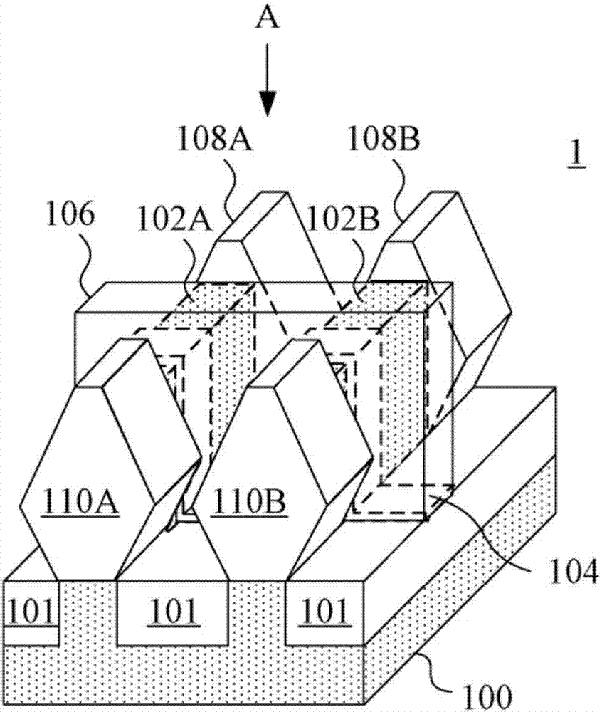
[0032] Please also refer to Figure 1A and Figure 1B . Figure 1A It is a three-dimensional view of a fin field effect transistor 1 in an embodiment of the present invention. Figure 1B In one embodiment of the present invention, Figure 1A The top view of the fin field effect transistor 1 along the direction A.

[0033] The FinFET 1 includes: a semiconductor substrate 100 , fin structures 102A, 102B, a gate dielectric layer 104 , a gate electrode structure 106 , drain structures 108A, 108B, and source structures 110A, 110B. It should be noted that, since the gate dielectric layer 104 is covered by the gate electrode structure 106, the Figure 1A and Figure 1B , the gate dielectric layer 104 is shown by a dotted line.

[0034] In one embodiment, the semiconductor substrate 100 is, for example, but not limited to a silicon substrate. The semiconductor substrate 100 includes a plurality of insulating regions 101 . The isolation region 101 includes structures such as, but n...


PUM


Abstract

A fin field-effect transistor includes a semiconductor substrate, fin structures, grid electrode dielectric layers, grid electrode structures, drain electrode structures and source electrode structures. The semiconductor substrate includes insulation zones. Each fin structure is arranged on the semiconductor substrate in an extending mode and is positioned between each two adjacent insulation zones. The grid electrode dielectric layers are disposed across each fin structure. The grid electrode structures are arranged on the grid electrode dielectric layers. The drain electrode structures are arranged on first sides, corresponding to the grid electrode structures, of the fin structures and have first resistance values with regard to the grid electrode structures. The source electrode structures are arranged on the second sides, corresponding to the grid electrode structures, of the fin structures and have second resistance values with regard to the grid electrode structures. The first resistance values are larger than the second resistance values.

Description

technical field [0001] The present invention relates to a semiconductor technology, and in particular to a fin field effect transistor (fin field effect transistor; FinFET) and a manufacturing method thereof. Background technique [0002] As the size of integrated circuits becomes smaller and the demand for higher driving capability increases, transistors need to be capable of generating high driving current with smaller and smaller sizes. Traditional transistors are prone to leakage current when the gate length is shrunk below 20 nanometers. Moreover, the shortening of the gate length makes the influence of the gate on the channel smaller. Under such circumstances, the FinFET with a three-dimensional source and drain structure has successfully overcome the above-mentioned problems and has become the mainstream of semiconductor technology in recent years. [0003] However, due to the small size, the FinFET cannot withstand high voltage at the semiconductor channel, making ...

Claims


Application Information

Patent Timeline
IPC IPC(8): H01L29/78H01L29/08H01L21/336
Inventor 叶达勋罗正玮颜孝璁简育生
Owner REALTEK SEMICON CORP
Features
  • R&D
  • Intellectual Property
  • Life Sciences
  • Materials
  • Tech Scout
  • Unparalleled Data Quality
  • Higher Quality Content
  • 60% Fewer Hallucinations
Learn More