Automatic adsorbing device used for array waveguide grating (AWG) and pasting method

An arrayed waveguide grating and adsorption device technology, which is applied to optical waveguides and light guides, etc., can solve the problems of increased clamping and coupling process difficulties, scrapped AWG chips, and high production costs, and can meet production process requirements, facilitate operation, and reduce labor costs. Effect

Inactive Publication Date: 2018-01-19
JIANGSU HENGTONG OPTICAL NETWORK TECH CO LTD +1
View PDF6 Cites 0 Cited by
  • Summary
  • Abstract
  • Description
  • Claims
  • Application Information

AI Technical Summary

Problems solved by technology

At the same time, due to the inherent characteristics of the curve of the AWG chip, and the influence of the AWG chip material (single crystal silicon) with high hardness, poor brittleness, and thin thickness, the clamping and coupling process of AWG device production is more difficult. In the process, due to improper operation, it is very easy to cause scrapping of AWG chips, resulting in high production costs

Method used


Image

  • Automatic adsorbing device used for array waveguide grating (AWG) and pasting method
  • Automatic adsorbing device used for array waveguide grating (AWG) and pasting method
  • Automatic adsorbing device used for array waveguide grating (AWG) and pasting method

Examples


Embodiment

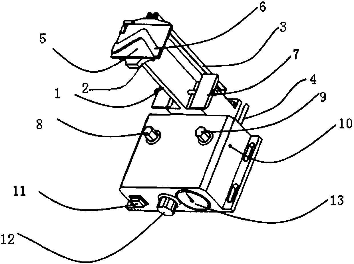
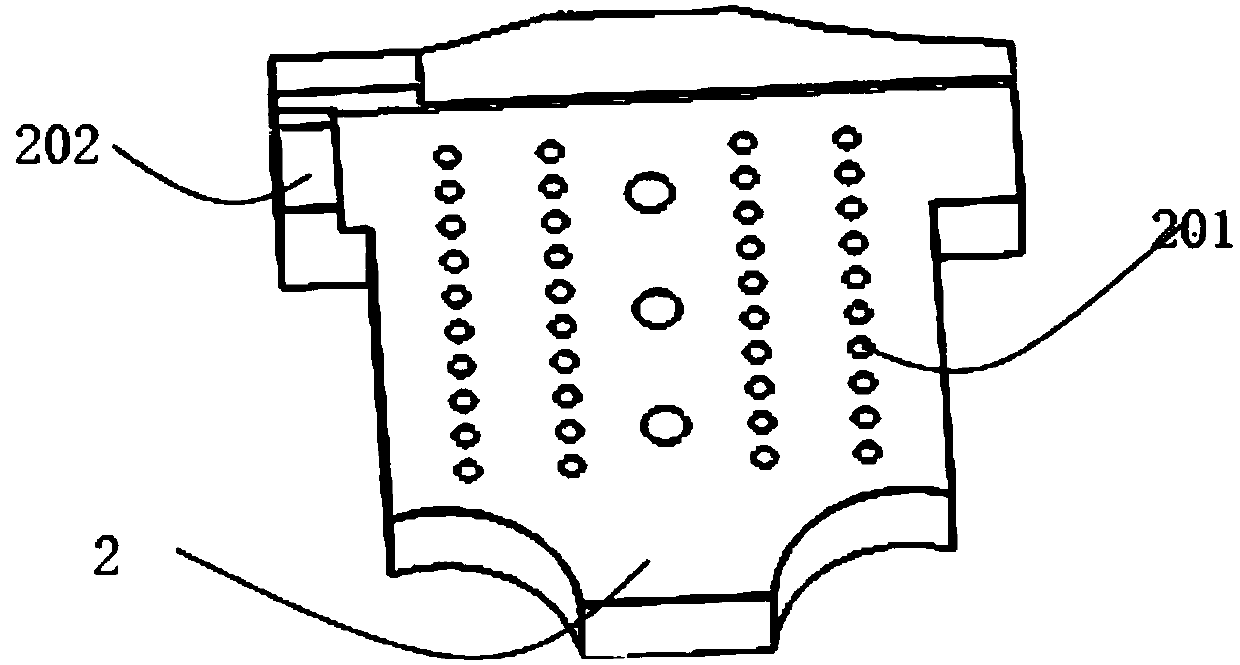
[0036] Such as Figure 1-5 As shown, this embodiment discloses an automatic adsorption device for arrayed waveguide gratings AWG. Its main structure includes: a central support 1, an adsorption platform 2, an air duct 3, and the adsorption platform 2 is arranged on the top of the central support 1. The air guide tube 3 is arranged on one side of the central support 1, one end of the above-mentioned air guide tube 3 is connected to the air pump source 4, and the other end of the above-mentioned air guide tube 3 is connected to the above-mentioned adsorption platform 2, and the above-mentioned adsorption platform 2 is provided with several air suction holes 201, the above-mentioned air guide tube 3 is connected with the above-mentioned suction holes 201, the number of the above-mentioned suction holes 201 can be an even number, and the above-mentioned suction holes are connected in pairs to ensure the uniformity of suction

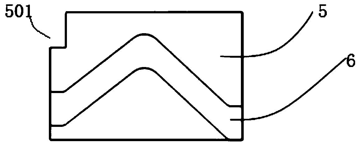
[0037] An optical quartz substrate 5 is detachably fix...


PUM


Abstract

The invention discloses an automatic adsorbing device used for an array waveguide grating (AWG). The automatic adsorbing device comprises a center support, an adsorbing platform and an air guide pipe,wherein the adsorbing platform is arranged at the top end of the center support, the air guide pipe is arranged at one side of the center support, one end of the air guide pipe is connected to an airpump source, and the other end of the air guide pipe is connected to the adsorbing platform; multiple suction holes are formed in the adsorbing platform, the air guide pipe is communicated with the suction holes, an optical quartz substrate is detachably fixed to the end face of the adsorbing platform, and an AWG chip is pasted on the upper surface of the optical quartz substrate. The automatic adsorbing device is simple in structure and convenient to operate and use, makes mass production easy, improves production efficiency and reduces material and manpower cost, and an electric system operates more stably.

Description

technical field [0001] The invention relates to the field of optical fiber communication, in particular to an automatic adsorption device and a pasting method for an arrayed waveguide grating (AWG). Background technique [0002] Arrayed waveguide grating (AWG) is an important optical device based on planar optical waveguide integration technology. With the rapid development of communication technology and its business, the research of large-capacity optical fiber communication system has great application value. Arrayed waveguide grating is the most ideal optical device to realize multi-channel dense wavelength division multiplexing optical network. It is also the basic optical communication technology for backbone optical transmission network and metropolitan core network. It has become the basis of optical communication network. It has wavelength multiplexing / demultiplexing functions, and wavelength multiplexing and demultiplexing devices are the basic devices of this tech...

Claims


Application Information

Patent Timeline
Patent Type & Authority Applications(China)
IPC IPC(8): G02B6/12
Inventor 施伟明陈立坚施雪磊施宇程孙权宋歆佳吴宏东
Owner JIANGSU HENGTONG OPTICAL NETWORK TECH CO LTD
Why Eureka
Try Eureka