Thin film transistor comprising light shielding layer, and preparation method of thin film transistor

A technology of thin-film transistors and light-shielding layers, which is applied in the direction of transistors, semiconductor/solid-state device manufacturing, and electric solid-state devices. It can solve problems such as circuit instability, increased circuit complexity, and power consumption, so as to improve efficiency and reduce photolithography steps. , The effect of simple preparation process steps

Inactive Publication Date: 2018-01-19
PEKING UNIV SHENZHEN GRADUATE SCHOOL
View PDF5 Cites 3 Cited by
  • Summary
  • Abstract
  • Description
  • Claims
  • Application Information

AI Technical Summary

Problems solved by technology

Although this method solves the influence of ambient light on the device to a certain extent, but also because the metal light-shielding layer has conductive properties, it needs to be connected to a fixed potential
If the fixed potential is not connected, the floating node will be added, and capacitive coupling will be introduced to cause circuit instability; if the fixed potential is increased, the complexity and power consumption of the circuit will be increased

Method used


Image

  • Thin film transistor comprising light shielding layer, and preparation method of thin film transistor
  • Thin film transistor comprising light shielding layer, and preparation method of thin film transistor
  • Thin film transistor comprising light shielding layer, and preparation method of thin film transistor

Examples


preparation example Construction

[0037] figure 2 It is a flowchart of a method for manufacturing a thin film transistor according to an embodiment of the present application.

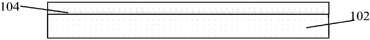
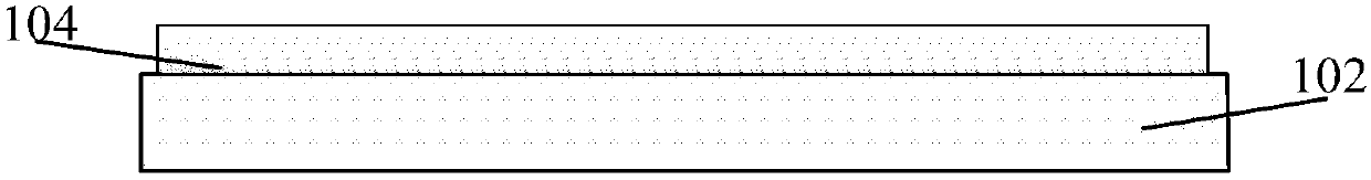
[0038] In S202, such as Figure 1a As shown, a layer of light-shielding layer 104 can be deposited on the substrate 102 first, such as Figure 1b The light shielding layer 104 is shown patterned. The substrate 102 may be a transparent material such as a glass substrate or a flexible substrate.

[0039]At present, metal materials are still used when preparing the light-shielding layer, although metal materials may have a series of defects. This is because, firstly, many non-metallic materials are transparent, and secondly, the light-shielding property is not the only requirement for the light-shielding layer material of the thin film transistor. To be used as a shading material also needs to meet the following series of requirements. It is beyond the reach of traditional technologies to find such a material that can be applied to ...


PUM


Abstract

The invention discloses a thin film transistor. The thin film transistor comprises a substrate, a patterned light shielding layer formed on the substrate, an active layer formed on the light shieldinglayer, a gate dielectric layer formed on the active layer and a gate electrode formed on the gate dielectric layer, and a passivation layer formed on the active layer and the gate electrode, whereinthe light shielding layer adopts an insulating non-metal light shielding material; and the active layer comprises a channel, a source region and a drain region of the transistor. The invention also provides a preparation method of the thin film transistor.

Description

technical field [0001] The present application relates to the preparation technology of thin film transistors, in particular to a thin film transistor including a light-shielding layer and a preparation method thereof. Background technique [0002] Display technology and industry is one of the fields with the most development potential in today's information technology and industry. The core of display technology is thin-film transistor (TFT) technology, and active matrix addressing flat panel displays such as liquid crystal display (Liquid Crystal Display, LCD) and organic light-emitting diode display (Organic Light-Emitting Diode, OLED) all rely on the control of TFT and drive. [0003] With the continuous improvement of display resolution and frame frequency, and even the use of TFTs for peripheral driving, the requirements for the driving ability of TFTs are getting higher and higher, and more and more researches on high-mobility oxide TFTs have attracted more and more ...

Claims


Application Information

Patent Timeline
Patent Type & Authority Applications(China)
IPC IPC(8): H01L21/336H01L29/786H01L27/32
Inventor 张盛东梁婷周晓梁卢慧玲张晓东王刚
Owner PEKING UNIV SHENZHEN GRADUATE SCHOOL
Why Eureka
Try Eureka