Wafer-level chip packaging structure and preparation method thereof

A wafer-level chip and packaging structure technology, applied in semiconductor/solid-state device manufacturing, electrical components, electrical solid-state devices, etc., can solve problems affecting the performance of packaged chips, low-k dielectric layer cracks, etc., to prevent damage and ensure performance Effect

Pending Publication Date: 2018-01-19
SJ SEMICON JIANGYIN CORP
View PDF5 Cites 3 Cited by
  • Summary
  • Abstract
  • Description
  • Claims
  • Application Information

AI Technical Summary

Problems solved by technology

[0003] In view of the above-mentioned shortcomings of the prior art, the object of the present invention is to provide a wafer-level chip packaging structure and its preparation method, which is used to solve the problem in the prior art that cracks will be generated in the low-k dielectric layer during the cutting process. , which in turn affects the performance of the packaged chip

Method used


Image

  • Wafer-level chip packaging structure and preparation method thereof
  • Wafer-level chip packaging structure and preparation method thereof
  • Wafer-level chip packaging structure and preparation method thereof

Examples


Embodiment 1

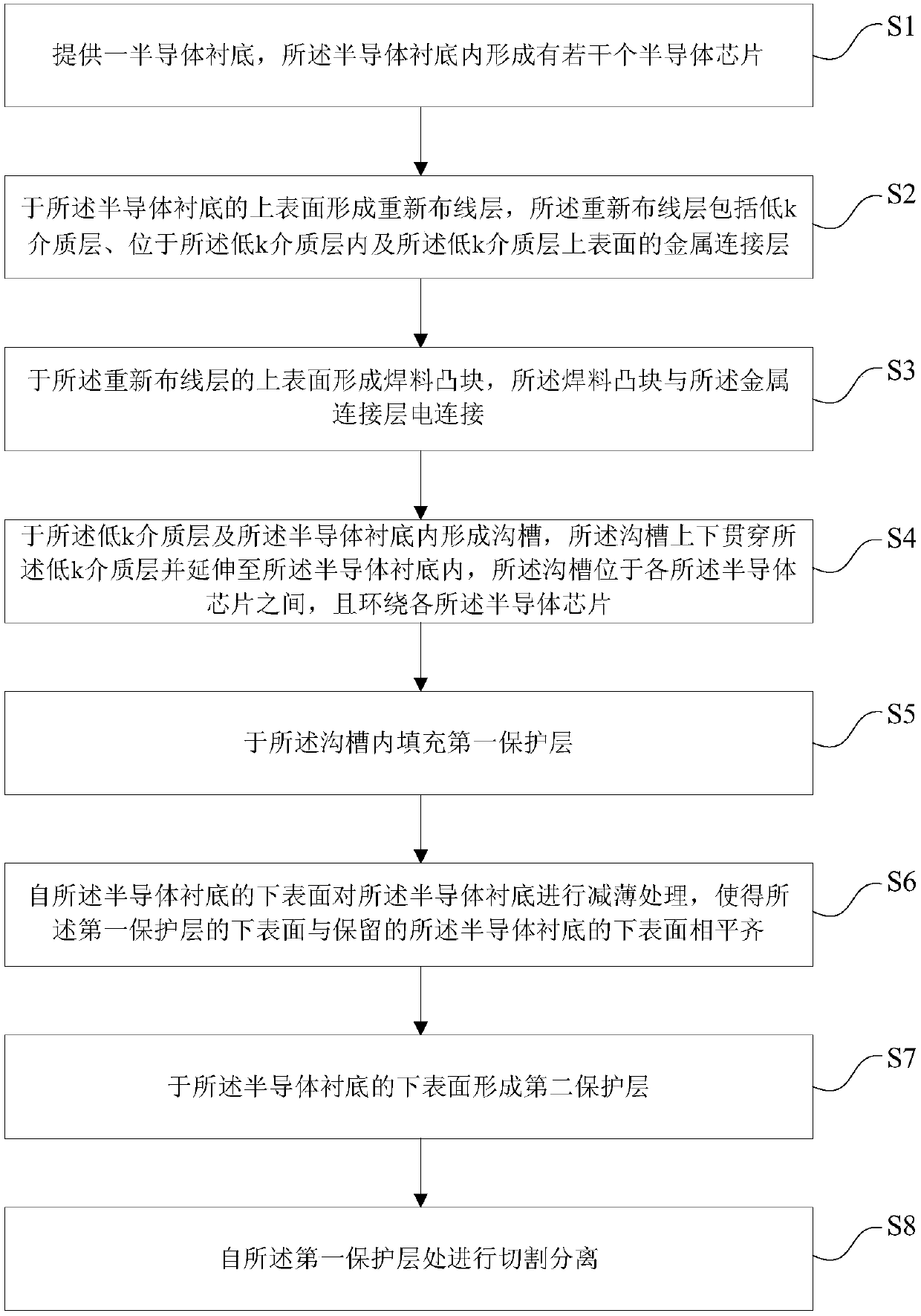
[0061] see figure 1 , the present invention provides a method for preparing a wafer-level chip packaging structure, the method for preparing the wafer-level chip packaging structure includes the following steps:

[0062] 1) providing a semiconductor substrate, in which several semiconductor chips are formed;

[0063] 2) forming a rewiring layer on the upper surface of the semiconductor substrate, the rewiring layer including a low-k dielectric layer, a metal connection layer located in the low-k dielectric layer and on the upper surface of the low-k dielectric layer;

[0064] 3) forming solder bumps on the upper surface of the rewiring layer, the solder bumps are electrically connected to the metal connection layer;

[0065] 4) forming trenches in the low-k dielectric layer and the semiconductor substrate, the trenches penetrate the low-k dielectric layer up and down and extend into the semiconductor substrate, and the trenches are located in each of the between and surroundin...

Embodiment 2

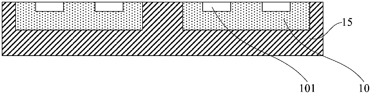
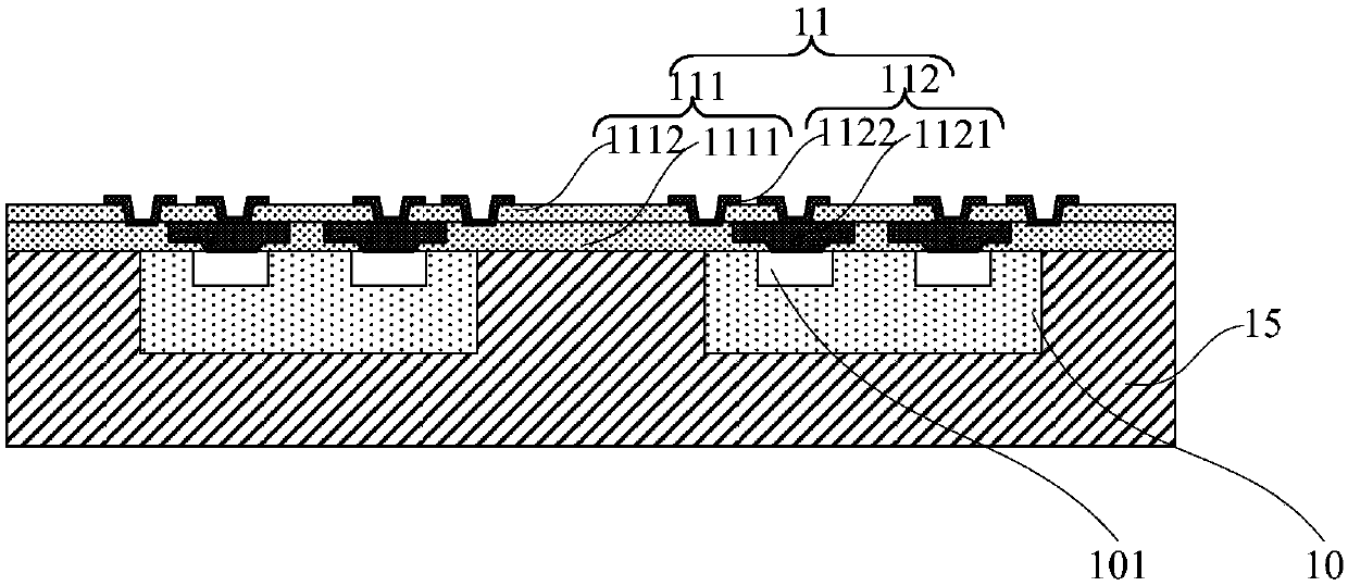
[0113] Please combine Figure 2 to Figure 10 read on Figure 11 , this embodiment also provides a wafer-level chip packaging structure, the wafer-level chip packaging structure includes: a semiconductor chip 10; a rewiring layer 11, the rewiring layer 11 includes a low-k dielectric layer 111, located The metal connection layer 112 in the low-k dielectric layer 111 and on the upper surface of the low-k dielectric layer 111; the low-k dielectric layer 111 is located on the front side of the semiconductor chip 10, and the metal connection layer 112 is connected to the semiconductor chip 10 electrical connection; solder bump 12, the solder bump 12 is located on the upper surface of the rewiring layer 11, and is electrically connected to the metal connection layer 112; the first protective layer 13, the first protective layer 13 Located on the periphery of the semiconductor chip and the rewiring layer 11 of the 10, and plastic-encapsulate the side of the semiconductor chip 10 and ...


PUM


Abstract

The invention provides a wafer-level chip packaging structure and a preparation method thereof. The wafer-level chip packaging structure comprises semiconductor chips, a rewiring layer, soldering fluxprotruding blocks, a first protecting layer and a second protecting layer, wherein the rewiring layer comprises low-k medium layers and metal connection layers located inside and on the upper surfaces of the low-k medium layers, and the soldering flux protruding blocks are located on the upper surface of the rewiring layer and electrically connected with the metal connection layers; the first protecting layer is located on the peripheries of the semiconductor chips and the periphery of the rewiring layer, and the second protecting layer is located on the back faces of the semiconductor chip and on the bottom of the first protecting layer. The first protecting layer is formed on the peripheries of the semiconductor chips and the periphery of the rewiring layer, in this way, it can be effectively avoided that external vapor permeates into the low-k medium layer, and the low-k medium layer is more prone to breaking, the low-k medium layer can be stabilized, external force is prevented from damaging the low-k medium layer, no cracks occur on the low-k medium layer during cutting, and then the performance of the packaged chips is ensured.

Description

technical field [0001] The invention relates to a semiconductor package structure and a package method, in particular to a wafer-level chip package structure and a preparation method thereof. Background technique [0002] In the existing wafer-level chip packaging structure (WLCSP), in order to meet the needs of small-scale development, low-k dielectric layers (such as rewiring layers) will be used in the wafer-level chip packaging structure, and subsequent Laser cutting (lasersaw) or blade cutting (blade saw); but because the low-k dielectric layer is relatively brittle, especially when the low-k dielectric layer is exposed to the atmospheric environment, after the water vapor in the atmosphere enters the low-k dielectric layer, so that all The above-mentioned low-k dielectric layer will easily generate cracks in the subsequent cutting process, and the presence of cracks in the low-k dielectric layer will seriously affect the performance of the packaged chip. Contents of ...

Claims


Application Information

Patent Timeline
Patent Type & Authority Applications(China)
IPC IPC(8): H01L23/00H01L23/31H01L23/488H01L21/98
CPCH01L2224/96H01L2224/04105H01L2224/12105H01L2224/18
Inventor 陈彦亨林正忠吴政达
Owner SJ SEMICON JIANGYIN CORP
Why Eureka
Try Eureka