
Method for forming ohmic contact and fabrication method of semiconductor device

A technology of ohmic contact and wafer, which is applied in semiconductor/solid-state device manufacturing, semiconductor devices, cleaning methods using liquids, etc., and can solve problems such as low device yield, rough ohmic contact surface, and high ohmic contact resistance

Active Publication Date: 2018-01-26
WUHAN XINXIN SEMICON MFG CO LTD
View PDF6 Cites 5 Cited by
  • Summary
  • Abstract
  • Description
  • Claims
  • Application Information

AI Technical Summary

Problems solved by technology

[0004] The object of the present invention is to provide a method for forming an ohmic contact and a method for manufacturing a semiconductor device, so as to solve the problems of rough ohmic contact surface, high ohmic contact resistance and low device yield in the prior art.

Method used


Image

  • Method for forming ohmic contact and fabrication method of semiconductor device
  • Method for forming ohmic contact and fabrication method of semiconductor device
  • Method for forming ohmic contact and fabrication method of semiconductor device

Examples


Embodiment Construction

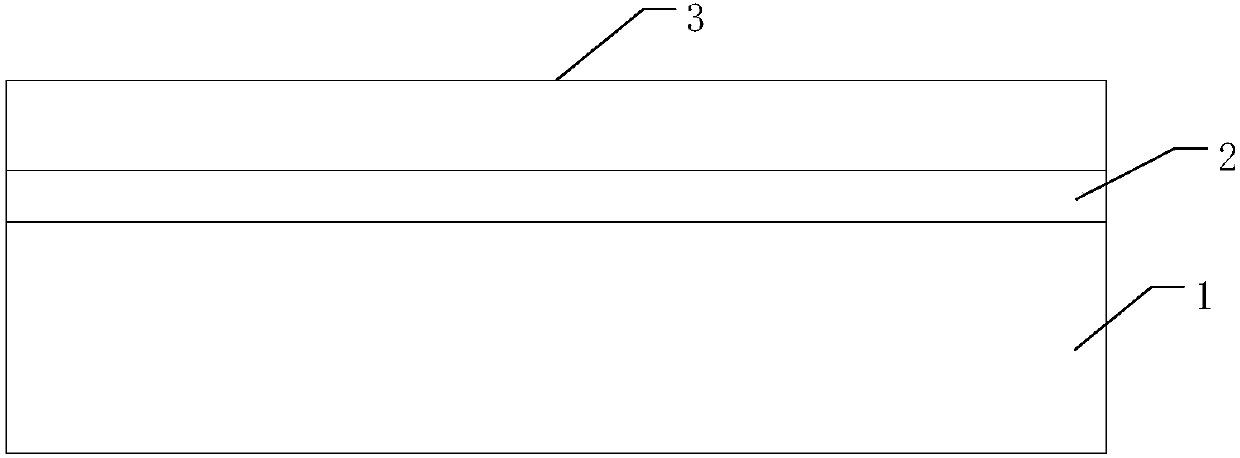
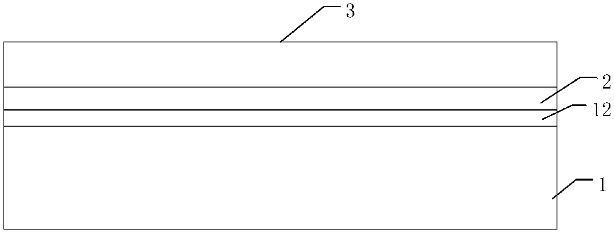
[0025] The specific implementation of the method for forming an ohmic contact provided by the present invention will be described in more detail below with reference to schematic diagrams. Advantages and features of the present invention will be apparent from the following description and claims. It should be noted that all the drawings are in a very simplified form and use imprecise scales, and are only used to facilitate and clearly assist the purpose of illustrating the embodiments of the present invention.

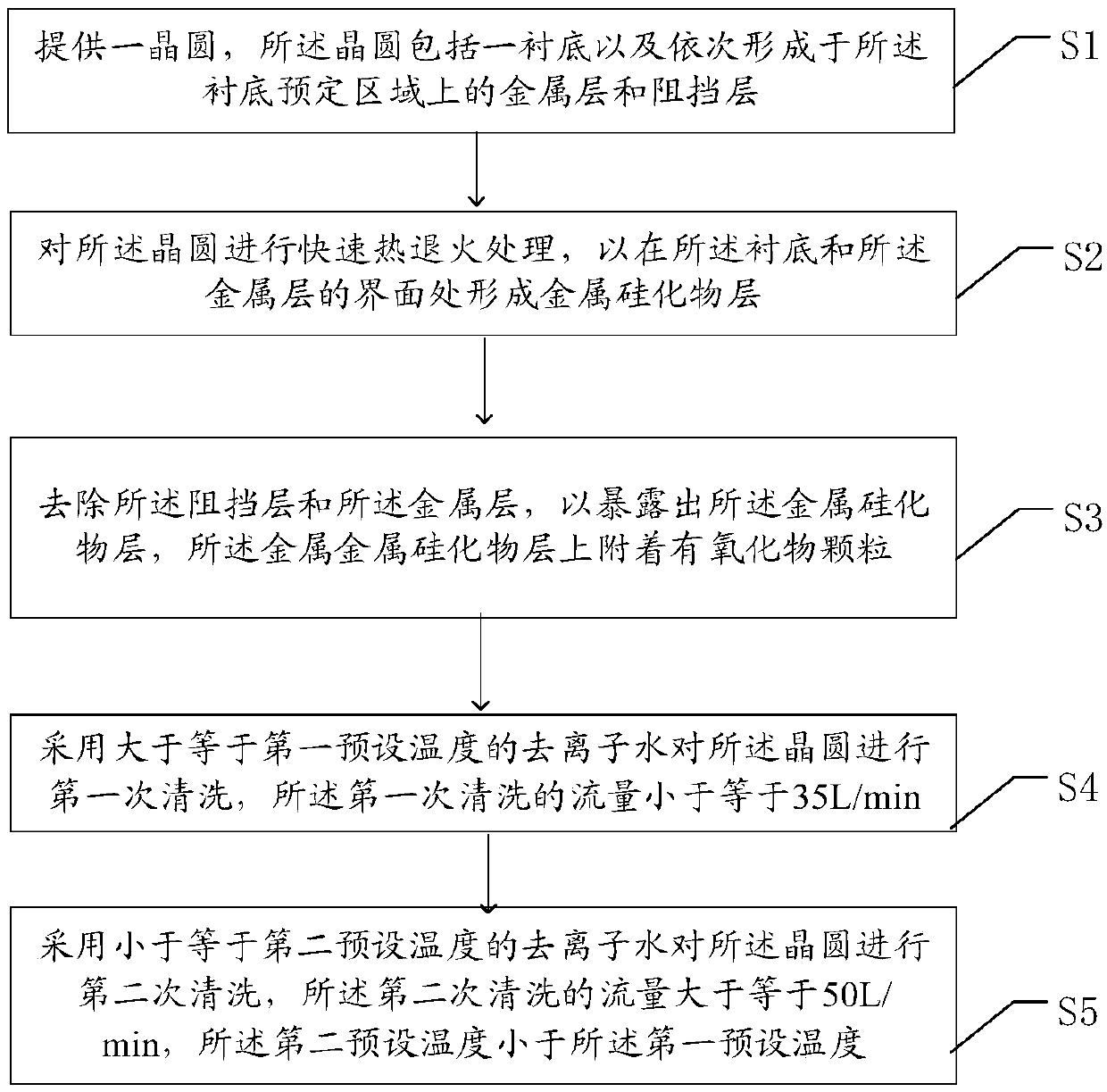
[0026] figure 1 The flow chart of the method for forming the ohmic contact provided by this embodiment, such as figure 1 As shown, the method for forming an ohmic contact includes:

[0027] S1: providing a wafer, the wafer includes a substrate and a metal layer and a barrier layer sequentially formed on a predetermined region of the substrate;

[0028] S2: performing rapid thermal annealing on the wafer to form a metal silicide layer at the interface between the sub...


PUM

PropertyMeasurementUnit
melting pointaaaaaaaaaa
thicknessaaaaaaaaaa
thicknessaaaaaaaaaa

Abstract

The present invention provides a method for forming ohmic contact. According to the method, after a metal silicide layer having thermal stability is formed, a barrier layer and a metal layer are removed, so that the metal silicide layer can be exposed; deionized water of which the temperature is larger than a first preset temperature is adopted to clean a wafer for the first time, so that oxide particles can be decomposed into small particles; deionized water of which the temperature is smaller than or equal to a second preset temperature is adopted to clean the wafer for the second time; andthe flow rate of the deionized water for the second cleaning is greater than 50L / min, the impact force of the water flow is large, so that the oxide particles can be removed. The water flows with different temperatures and different flow rates are utilized to wash the wafer, so that a better cleaning effect can be realized, and therefore, the oxide particles on the metal silicide layer can be removed, the oxide particles on the metal silicide layer are effectively reduced, and thus, an ohmic contact surface is smoothened, and the reliability and yield of a device can be improved.

Description

technical field [0001] The invention relates to the field of semiconductor manufacturing, in particular to a method for forming an ohmic contact and a method for manufacturing a semiconductor device. Background technique [0002] Ohmic contact is a key process technology in semiconductor manufacturing. Its purpose is to make the voltage drop at the contact of the semiconductor material small enough to not affect the performance of the device when a voltage is applied. If the reliability of the ohmic contact resistance is poor, the on-state resistance of the device will increase, and in severe cases, the performance of the device will be affected. [0003] In existing chip designs, ohmic contacts usually use special refractory metals as contacts on the surface of silicon to reduce resistance and enhance adhesion. However, the ohmic contact surface formed in the subsequent process is very rough, so the ohmic contact resistance is high, and even fails, so that the reliability ...

Claims


Application Information

Patent Timeline
Patent Type & Authority Applications(China)
IPC IPC(8): H01L21/02H01L21/28H01L29/45B08B3/02
Inventor 杨德林
Owner WUHAN XINXIN SEMICON MFG CO LTD
Learn More