


Quick Research
Generate reliable direction feasibility study reports for your R&D in just a few steps.

Technical Q&A
Discover and master advanced knowledge NOW. Basics, ideas, possibilities, all at once.

Find Solutions
As an expert in R&D theories, this can generate solutions to your technical problems instantly.

Evaluate Feasibility
Analyze your overall solution with one click, know your potential R&D risks in advance.

Monitor Landscape
Get weekly tech updates, stay abreast of the latest tech innovations and key insights.
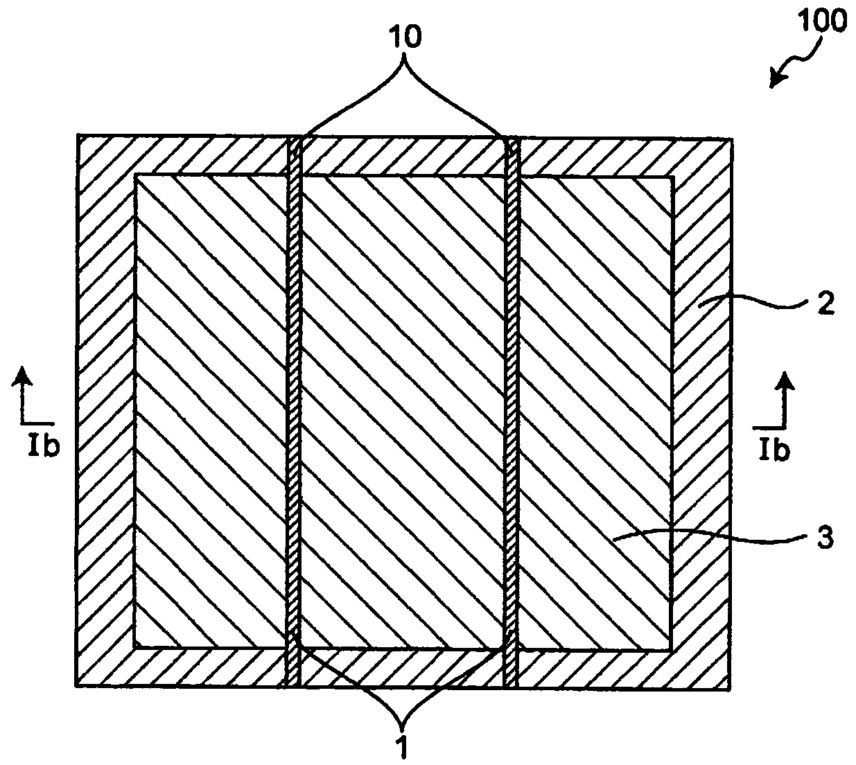
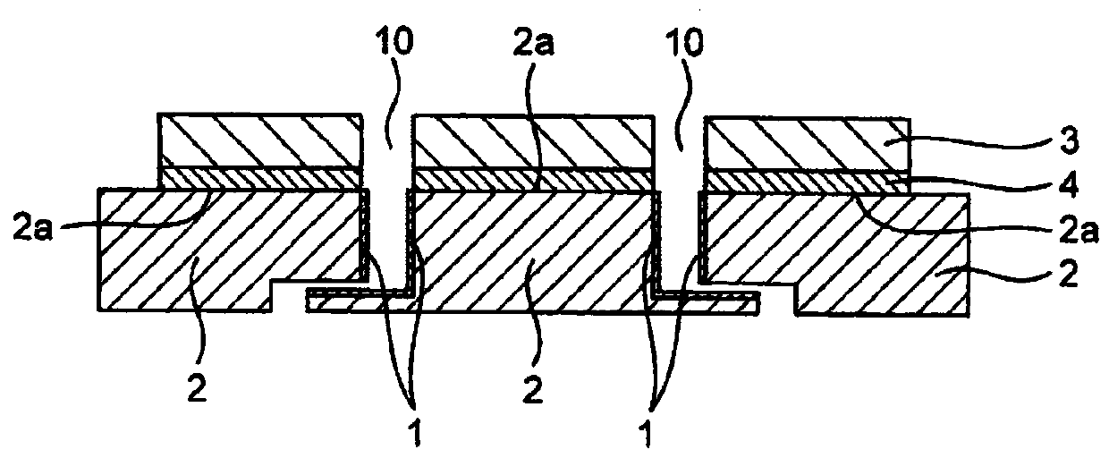
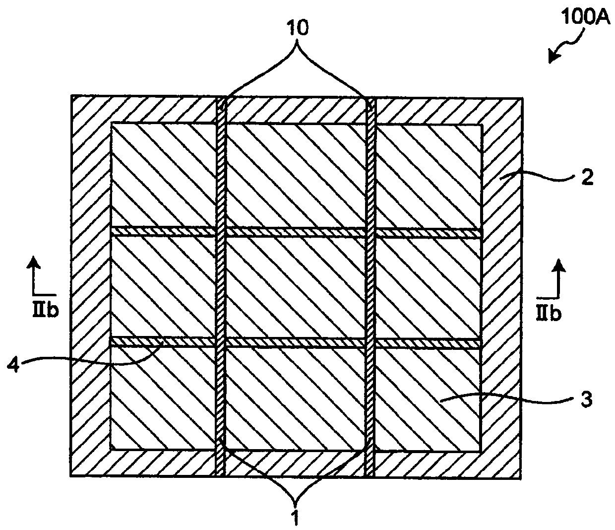
Sputtering target assembly
A sputtering target and assembly technology, which is applied in sputtering coating, metal material coating process, semiconductor/solid-state device manufacturing, etc., and can solve problems such as difficulty in large-scale
- Summary
- Abstract
- Description
- Claims
- Application Information
AI Technical Summary
Problems solved by technology
Method used
Image

Examples
Embodiment
[0088] Hereinafter, the present invention is described in more detail by enumerating the examples, but the present invention is not limited by the following examples, and can also be modified and implemented within the scope of meeting the stated and hereinafter-described gist, and these changes are all included in the present invention within the technical range.
[0089] In this embodiment, the case where there is a coating (electroless Ni-P plating film, electrolytic Ni plating film, or Cr plating film) in the gap portion 10 between adjacent mounting parts 2a, and the case where there is no coating The influence of the state of the layer on the properties of the oxide semiconductor thin film was investigated.
[0090] make Figure 3A and Figure 3B A base plate 2 made of pure Cu is shown with gaps 10 . More specifically, the bottom plate 2 has a diameter of 126 mm and a thickness of 7 mm (thickness of the portion having the mounting portion 2 a ), and the width of the ga...
PUM
 Abstract
Description
Claims
Application Information
 - R&D Engineer
- R&D Manager
- IP Professional
- Industry Leading Data Capabilities
- Powerful AI technology
- Patent DNA Extraction
Browse by: Latest US Patents, China's latest patents, Technical Efficacy Thesaurus, Application Domain, Technology Topic, Popular Technical Reports.
© 2024 PatSnap. All rights reserved.Legal|Privacy policy|Modern Slavery Act Transparency Statement|Sitemap|About US| Contact US: help@patsnap.com