Circuit-embedded type single-sided flexible circuit board and preparation method thereof

A flexible circuit board and embedded technology, which is applied in the fields of printed circuit manufacturing, printed circuit, printed circuit components, etc., can solve problems such as the inability to meet the needs of low line spacing circuit boards, reduce the risk of short circuit in the package, and improve assembly , good bending effect

Active Publication Date: 2018-01-30
AKM ELECTRONICS TECH SUZHOU
View PDF3 Cites 2 Cited by
  • Summary
  • Abstract
  • Description
  • Claims
  • Application Information

AI Technical Summary

Problems solved by technology

The minimum pitch (the distance between the center points of two adjacent circuits) produced in the traditional subtractive process in the prior art is 60 μm, but most of the ones that can be mass-produced are 70 μm; the limit of the semi-additive process 40μm, most of which can be mass-produced are 50μm, but it still cannot meet the market's demand for low line spacing circuit boards

Method used


Image

  • Circuit-embedded type single-sided flexible circuit board and preparation method thereof
  • Circuit-embedded type single-sided flexible circuit board and preparation method thereof
  • Circuit-embedded type single-sided flexible circuit board and preparation method thereof

Examples


Embodiment 1

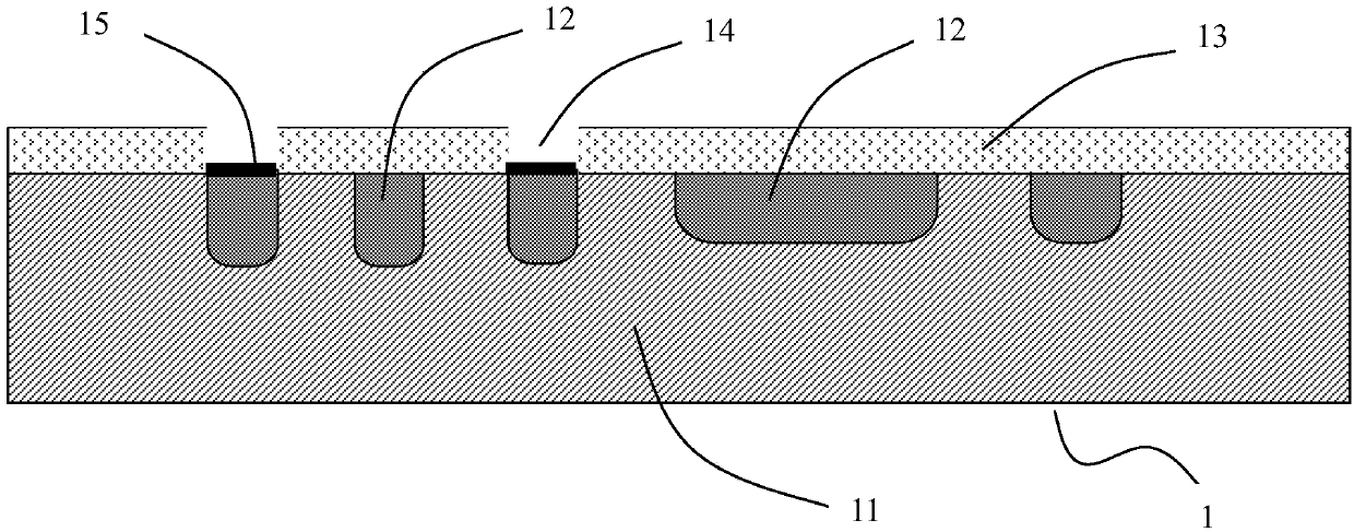
[0039] see Figure 1 to Figure 9 , a single-sided flexible circuit board 1 of the present embodiment includes an insulating layer 11 and a circuit 12 embedded in the insulating layer 11. There are several pad areas 14 on the circuit 12, and the upper surface of the circuit 12 in the pad area 14 has The surface treatment layer 15 has a solder resist layer 13 on the upper surface of the circuit 12 except the pad region 14 and the upper surface of the insulating layer 11 . In this embodiment, the material of the insulating layer 11 is polyimide (PI), the material of the solder resist layer 13 is solder resist ink, and the surface treatment layer is a metal plating layer, which is a gold layer, a palladium layer and a nickel layer from top to bottom. , the thickness is 0.05-0.15 μm, 0.05-0.15 μm, 3-8 μm in turn.

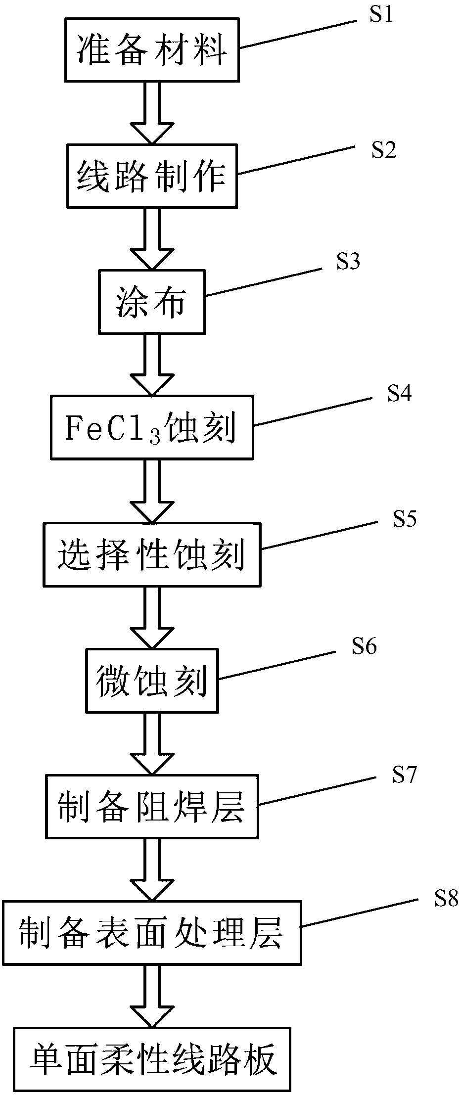
[0040] This embodiment also provides a method for preparing a single-sided flexible circuit board, such as figure 2 As shown, it specifically includes the following s...

Embodiment 2

[0060] see Figure 1 to Figure 8 and Figure 10 to Figure 12 , a single-sided flexible circuit board 1 of the present embodiment includes an insulating layer 11 and a circuit 12 embedded in the insulating layer 11. There are several pad areas 14 on the circuit 12, and the upper surface of the circuit 12 in the pad area 14 has The surface treatment layer 15 has a solder resist layer 13 on the upper surface of the circuit 12 except the pad region 14 and the upper surface of the insulating layer 11 . In this embodiment, the material of the insulating layer 11 is polyimide (PI), the material of the solder resist layer 13 is polyimide, and the surface treatment layer is a metal plating layer, which is a gold layer, a palladium layer and a nickel layer from top to bottom. layer, the thickness is 0.05-0.15 μm, 0.05-0.15 μm, 3-8 μm in sequence.

[0061] This embodiment also provides a method for preparing a single-sided flexible circuit board, such as Figure 10 As shown, it specif...


PUM


Abstract

The invention discloses a circuit-embedded type single-sided flexible circuit board comprising an insulating layer and a circuit embedded in the insulating layer. A plurality of bonding pad areas areformed at the circuit; surface treatment layers are formed on the upper surface of the circuit in the bonding pad areas; and solder mask layers are formed on the upper surface of the circuit except the bonding pad areas and the upper surface of the insulating layer. According to the invention, the circuit of the single-sided flexible circuit board is embedded into the insulating layer, so that thehigh reliability is kept and the width and line spacing of the circuit are reduced; the product is extremely thin; the bending and assembling properties are good; and the packaging short-circuit riskof the client is reduced. In addition, the preparation method of the single-sided flexible circuit board has advantages of low cost and high reliability and is easy to realize; and batched productionis realized.

Description

technical field [0001] The invention belongs to the technical field of printed circuits, and in particular relates to a line-embedded single-sided flexible circuit board and a preparation method thereof. Background technique [0002] With the continuous advancement of science and technology, the consumer electronics industry such as mobile phones, Pads and other products are developing rapidly, and the demand for miniaturization and high resolution of the display screen is becoming more and more urgent, thus increasing the requirements for the fineness of the circuit of the flexible board package carrier board. Require. The minimum pitch (the distance between the center points of two adjacent circuits) produced in the traditional subtractive process in the prior art is 60 μm, but most of the mass production can be achieved with 70 μm; the semi-additive process limit 40μm, most of which can be mass-produced are 50μm, but it still cannot meet the market's demand for low-pitch...

Claims


Application Information

Patent Timeline
Patent Type & Authority Applications(China)
IPC IPC(8): H05K3/18H05K3/24H05K3/28H05K1/02H05K1/11
Inventor 邓明黄大兴李大树张子龙
Owner AKM ELECTRONICS TECH SUZHOU
Why Eureka
Try Eureka