Electron diffractometer capable of realizing automatic defect regulation

An electron diffraction and defect technology, applied in the field of electron diffractometer, can solve the problems of effective control of difficult-to-grow defects

Active Publication Date: 2018-02-02
WUHAN UNIV
View PDF4 Cites 9 Cited by
  • Summary
  • Abstract
  • Description
  • Claims
  • Application Information

AI Technical Summary

Problems solved by technology

[0006] The purpose of the present invention is to provide an electron diffractometer that can realize the automatic control of defects, aim

Method used


Image

  • Electron diffractometer capable of realizing automatic defect regulation

Examples


Embodiment Construction

[0022] The following will clearly and completely describe the technical solutions in the embodiments of the present invention with reference to the accompanying drawings in the embodiments of the present invention. Obviously, the described embodiments are only some, not all, embodiments of the present invention. Based on the embodiments of the present invention, all other embodiments obtained by persons of ordinary skill in the art without making creative efforts belong to the protection scope of the present invention.

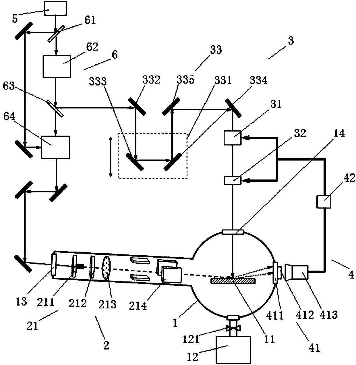
[0023] see figure 1 , the embodiment of the present invention provides an electronic diffractometer that can realize automatic control of defects, including a vacuum sample chamber 1, a sample stage 11 is arranged in the vacuum sample chamber 1, and samples can be prepared on the sample stage 11, mainly for crystal materials Heteroepitaxial growth, such as the growth of layered films, for the vacuum sample chamber 1, it is mainly to ensure that the sample prep...


PUM

PropertyMeasurementUnit
Angle of incidenceaaaaaaaaaa
Center wavelengthaaaaaaaaaa
Diameteraaaaaaaaaa

Abstract

The invention relates to an electron diffractometer and provides an electron diffractometer capable of realizing automatic defect regulation. The electron diffractometer comprises a vacuum sample room, and also comprises a testing optical path, a detect regulation optical path and a processing unit. Frequency tripled laser of the testing optical path is transmitted from a first incidence window into the vacuum sample room. Frequency doubled laser of the defect regulation optical path is transmitted from a second incidence window into a sample stage inside the vacuum sample room. An electronicgun is also arranged inside the vacuum sample room. A cathode of the electronic gun is positioned on the testing optical path. The defect regulation optical path is provided with a laser pulse energyregulator and a laser pulse scanning device. The processing unit comprises a receiving component and a control center. The electron diffractometer of the invention can achieve in-situ real-time nondestructive measurement of the micro- and nano-fabrication process and realize growth while testing. In addition, sample surface defect information is obtained through processing of diffraction images, and femtosecond laser pulse energy and scanning position are regulated according to the invention so as to repair defects, thus achieving the purpose of testing while regulating.

Description

technical field [0001] The invention relates to an electron diffractometer, in particular to an electron diffractometer capable of automatic control of defects. Background technique [0002] Advanced micro-nano manufacturing technology, as a primitive productivity, promotes the progress of society, and thin film growth represents one of the main development directions of advanced micro-nano manufacturing. Typical representatives of thin film growth include chemical vapor deposition, molecular beam epitaxy, pulsed laser deposition, ultrafast laser micro-nano processing, electron pulse exposure, focused ion beam, nano welding / connection, etc., including thin film crystal growth, surface micro-nano composite structure, Two-dimensional material preparation and other manufacturing methods are emerging industries such as power electronics, display, semiconductor lighting, bionic materials, micro-mechanics, micro-nano electronics, optoelectronics, electronic packaging, new solar en...

Claims


Application Information

Patent Timeline
IPC IPC(8): G01N23/20058G01N23/20025
CPCG01N23/20025G01N23/20058G01N2223/0565G01N2223/307G01N2223/646
Inventor 刘胜李辉张国庆申胜男
Owner WUHAN UNIV
Why Eureka
Try Eureka