Double-module layer-by-layer measuring system

A technology for measuring systems and components, applied in the field of electron diffractometers, can solve problems such as regulation and difficult growth defects

Active Publication Date: 2017-12-12
WUHAN UNIV
View PDF4 Cites 5 Cited by
  • Summary
  • Abstract
  • Description
  • Claims
  • Application Information

AI Technical Summary

Problems solved by technology

[0008] The purpose of the present invention is to provide a dual-mode layer-by-layer measurement system, which aims to solve the problem that it is difficult to effectively control growth defects in the existing thin film manufacturing technology

Method used


Image

  • Double-module layer-by-layer measuring system

Examples


Embodiment Construction

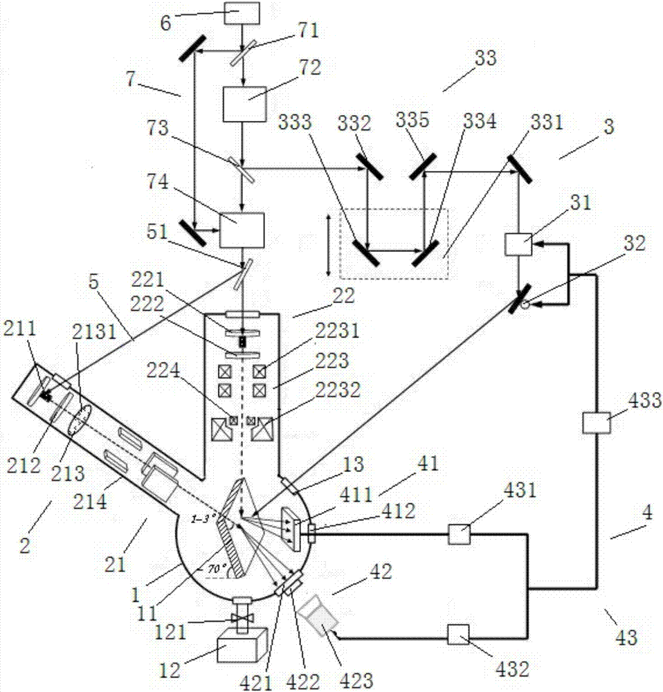
[0024] The following will clearly and completely describe the technical solutions in the embodiments of the present invention with reference to the accompanying drawings in the embodiments of the present invention. Obviously, the described embodiments are only some, not all, embodiments of the present invention. Based on the embodiments of the present invention, all other embodiments obtained by persons of ordinary skill in the art without making creative efforts belong to the protection scope of the present invention.

[0025] see figure 1, the embodiment of the present invention provides a dual-mode layer-by-layer measurement system, including a vacuum sample chamber 1, a sample stage 11 is arranged in the vacuum sample chamber 1, and samples can be prepared on the sample stage 11, mainly for crystal material heteroepitaxial Growth, such as the growth of layered films, for the vacuum sample chamber 1, it is mainly to ensure that the sample preparation environment is in a vac...


PUM


Abstract

The invention relates to an electron diffractometer, and provides a double-module layer-by-layer measuring system. The double-module layer-by-layer measuring system comprises a vacuum sample chamber, wherein the vacuum sample chamber is internally provided with a sample platform; and further comprises an electronic impulse control unit, a defect regulating and controlling light path and a processing unit, wherein the defect regulating and controlling light path is provided with a laser pulse energy regulating device and a laser pulse scanning device, and the processing unit comprises a first receiving component for receiving an electronic back scattering pattern, a second receiving component for receiving a diffraction image and a control center for analyzing the received diffraction image and the electronic back scattering pattern so as to control the laser pulse energy regulating device and the laser pulse scanning device. The measuring system is capable of realizing the in-situ real-time nondestructive measurement for the micro-nano manufacturing process, simultaneously realizing the growth and detection, receiving sample surface defect information through processing the diffraction image and the back scattering pattern, and regulating the femtosecond laser pulse energy and scanning position according to the information feedback. The defect is repaired, and the purpose of simultaneously detecting and regulating can be realized.

Description

technical field [0001] The invention relates to an electron diffractometer, in particular to a dual-mode layer-by-layer measurement system. Background technique [0002] Advanced micro-nano manufacturing technology, as a primitive productivity, promotes the progress of society, and thin film growth represents one of the main development directions of advanced micro-nano manufacturing. Typical representatives of thin film growth include chemical vapor deposition, molecular beam epitaxy, pulsed laser deposition, ultrafast laser micro-nano processing, electron beam exposure, focused ion beam, nano welding / connection, etc., including thin film crystal growth, surface micro-nano composite structure, Two-dimensional material preparation and other manufacturing methods are emerging industries such as power electronics, display, semiconductor lighting, bionic materials, micro-mechanics, micro-nano electronics, optoelectronics, electronic packaging, new solar energy, low-dimensional ...

Claims


Application Information

Patent Timeline
Patent Type & Authority Applications(China)
IPC IPC(8): G01N23/20G01N23/203
CPCG01N23/20G01N23/203
Inventor 刘胜李辉张国庆申胜男
Owner WUHAN UNIV
Why Eureka
Try Eureka