Printed circuit board assembly and terminal device

A technology for printed circuit boards and terminal equipment, which is applied to printed circuit components, structural connections of printed circuits, circuit devices, etc. It can solve problems such as waste of internal space on the motherboard, complex internal environment of the PCB, and increased design costs. Effects of design cost, shortened R&D cycle, and wide trace width

Pending Publication Date: 2018-02-16
MEIZU TECH CO LTD
View PDF0 Cites 3 Cited by
  • Summary
  • Abstract
  • Description
  • Claims
  • Application Information

AI Technical Summary

Problems solved by technology

[0003] 1. As the thickness of the PCB becomes thinner, the thickness of the insulating layer and the thickness of the copper of the multi-layer PCB board also decrease accordingly, which makes the high-frequency impedance line of the RF module need a thinner line width to achieve 50 ohm impedance Requirements, however, the too thin line width exceeds the process capability of the conventional process, which requires the use of new insulating materials or new process technology, which greatly increases the design cost;
[0004] 2. In the design of the mobile phone PCB motherboard, the radio frequency area needs to be laid out separately from other module

Method used


Image

  • Printed circuit board assembly and terminal device
  • Printed circuit board assembly and terminal device
  • Printed circuit board assembly and terminal device

Examples


Embodiment Construction

[0048] In order to understand the above-mentioned purpose, features and advantages of the present invention more clearly, the present invention will be further described in detail below in conjunction with the accompanying drawings and specific embodiments. It should be noted that, in the case of no conflict, the embodiments of the present application and the features in the embodiments can be combined with each other.

[0049] In the following description, many specific details are set forth in order to fully understand the present invention. However, the present invention can also be implemented in other ways than described here. Therefore, the protection scope of the present invention is not limited by the specific implementation disclosed below. Example limitations.

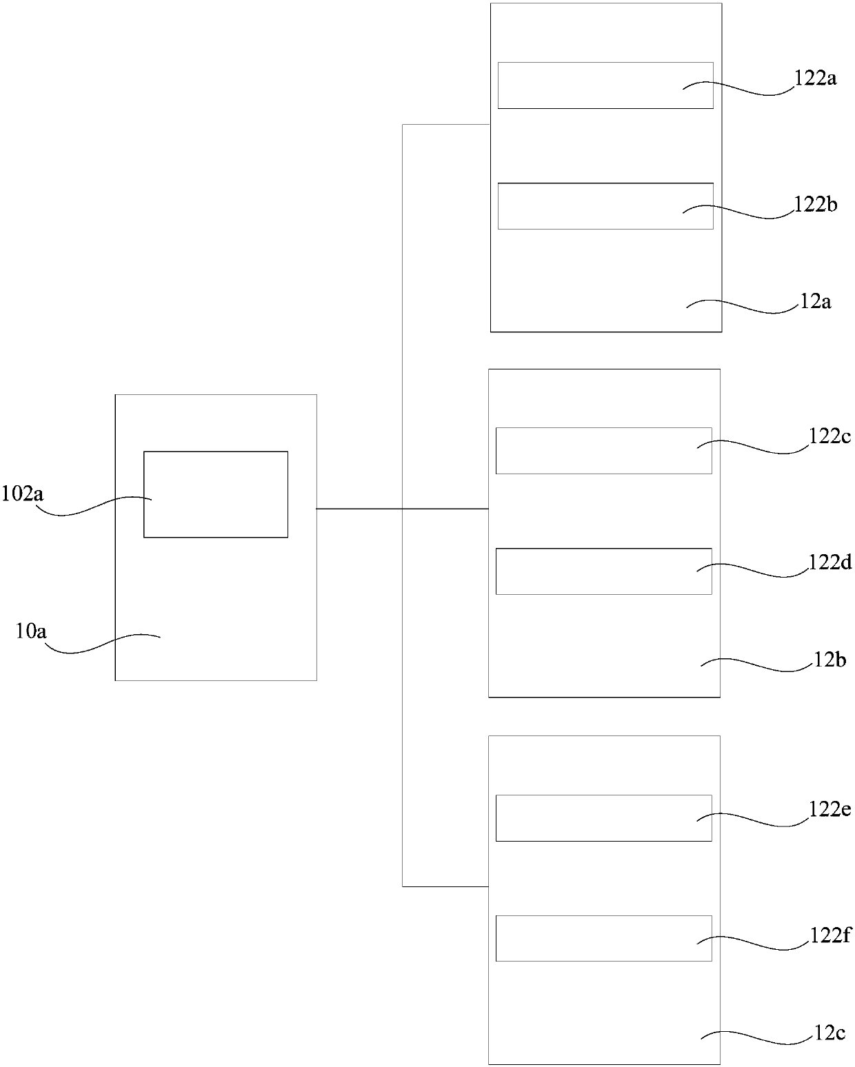
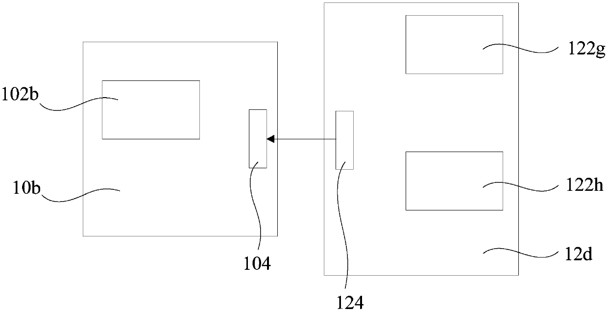
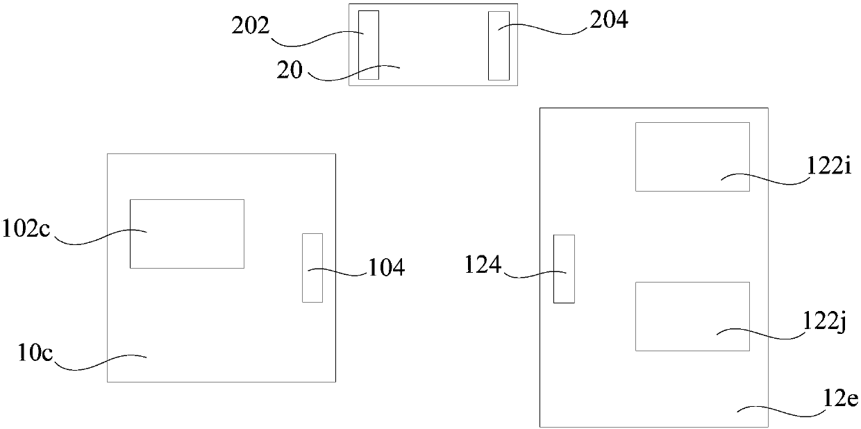
[0050] In an embodiment of the first aspect of the present invention, a printed circuit board assembly is proposed, figure 1 A schematic diagram showing a printed circuit board assembly according to an embod...


PUM


Abstract

The present invention provides a printed circuit board assembly and a terminal device, wherein the printed circuit board assembly includes: a first printed circuit board; a radio frequency module arranged on the first printed circuit board; at least one second printed circuit board On the circuit board, at least one first-type functional module is arranged on at least one second printed circuit board, and the second printed circuit board is connected to the first printed circuit board. The printed circuit board assembly provided by the present invention makes the design of the printed circuit board assembly more flexible by separating the radio frequency module and the first type of functional module, and avoids the waste caused by the design of the radio frequency module and the PCB main board on the same board. The design cost is reduced, the loss on the routing of the radio frequency signal is reduced, the development cycle can be shortened, and the influence of noise on the performance of the radio frequency signal can be avoided.

Description

technical field [0001] The present invention relates to the technical field of electronic equipment, in particular to a printed circuit board assembly and terminal equipment. Background technique [0002] Currently, in the design of a printed circuit board (PCB) of a smart phone, a radio frequency module, a processor (Application Processor, AP) module and other functional modules are all located on the same PCB main board. However, with more and more mobile phone functions, the main board of the mobile phone is getting thinner and thinner, which makes the PCB design of the RF module face the following problems: [0003] 1. As the thickness of the PCB becomes thinner, the thickness of the insulating layer and the thickness of the copper of the multi-layer PCB board also decrease accordingly, which makes the high-frequency impedance line of the RF module need a thinner line width to achieve 50 ohm impedance Requirements, however, the too thin line width exceeds the process ca...

Claims


Application Information

Patent Timeline
IPC IPC(8): H05K1/02H05K1/14
CPCH05K1/0216H05K1/14
Inventor 张利科
Owner MEIZU TECH CO LTD
Why Eureka
Try Eureka