
Semiconductor package

A semiconductor and active surface technology, applied in semiconductor devices, semiconductor/solid-state device manufacturing, semiconductor/solid-state device components, etc., can solve problems such as high packaging failure rate and collapse, and achieve the effect of avoiding excessive collapse

Inactive Publication Date: 2018-02-23
CHIPMOS TECH INC
View PDF3 Cites 0 Cited by
  • Summary
  • Abstract
  • Description
  • Claims
  • Application Information

AI Technical Summary

Problems solved by technology

However, if the wettability of the trace is too good, the bump may flow along the trace and collapse when it is bonded with the trace by reflow soldering, resulting in a rather high package failure rate

Method used


Image

  • Semiconductor package
  • Semiconductor package
  • Semiconductor package

Examples


Embodiment Construction

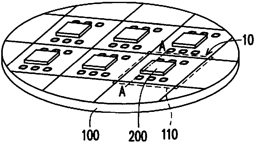
[0036] Figure 1A is a schematic diagram of a semiconductor package according to an embodiment of the present invention. Please see first Figure 1A , Figure 1A It shows a plurality of semiconductor packages 10 that have not been cut, and a wafer 100 located below includes a plurality of first chips 110 arranged in an array, and a plurality of second chips 200 are respectively flip-chip configured on the first chips 110 of the wafer 100 superior.

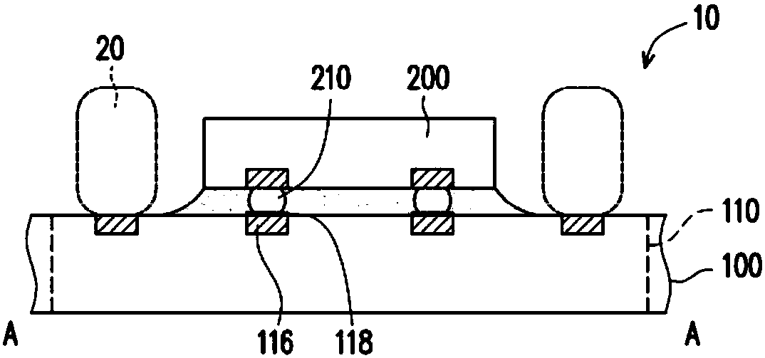
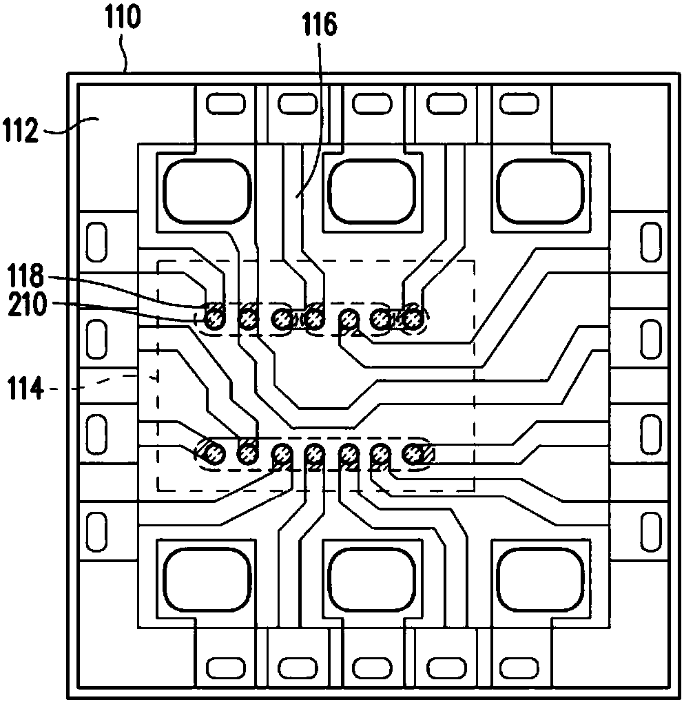
[0037] Figure 1B is along Figure 1A A schematic cross-sectional view of the A-A line segment. figure 2 yes Figure 1A An enlarged schematic top view of one of the semiconductor packages in . It should be noted that in figure 2 The second chip 200 and the encapsulant between the first chip 100 and the second chip 200 are intentionally hidden in order to expose the relative positions between the bumps 210 and the wires 116 . see Figure 1B to Figure 2 , the semiconductor package 10 of this embodiment includes a first chip 11...


PUM


Abstract

The present invention provides a semiconductor package including a first chip and a second chip. The first chip includes a first active surface, wherein the first active surface includes a bonding area, a plurality of traces extending into the bonding area, and a plurality of high-humidity pads disposed on the traces, wherein the high-humidity pads are configured These traces are localized in thejunction area. The second chip is flip-chiply disposed on the bonding area of the first chip and includes a plurality of bumps, wherein the bumps connect the high-wetting pads of the traces, and between the high-wetting pads and the bumps. The degree of wetting is greater than the degree of wetting between the other parts of these traces and these bumps, respectively. The semiconductor package provided by the present invention has a bump on one chip that can be well bonded to the trace of another chip and still has a certain height.

Description

technical field [0001] The invention relates to a package, in particular to a semiconductor package. Background technique [0002] With the rapid development of technology, integrated circuits (IC) components have been widely used in our daily life. Generally speaking, the production of integrated circuits is mainly divided into three stages: the manufacture of silicon wafers, the fabrication of integrated circuits and the packaging of integrated circuits. [0003] In the current packaging structure, it is a fairly common packaging type to bond a chip to another chip or to the traces of a wafer through bumps in a flip-chip manner. Generally speaking, the above-mentioned traces are made of materials with high stability, good ductility, and good wetting, such as gold, for yield, production efficiency, wire diameter miniaturization, and the gap between bumps. Good performance on joints. However, if the wettability of the traces is too good, the bumps may flow along the trace...

Claims


Application Information

Patent Timeline
IPC IPC(8): H01L21/60H01L23/48
CPCH01L23/48H01L24/17H01L24/49H01L2224/171H01L2224/17104H01L2224/491H01L2224/73204
Inventor 黄东鸿翁承谊
Owner CHIPMOS TECH INC
Learn More